Apparatus and method of digital imaging on a semiconductor substrate

Inactive Publication Date: 2006-02-09
AVAGO TECH WIRELESS IP SINGAPORE PTE
View PDF2 Cites 21 Cited by
  • Summary
  • Abstract
  • Description
  • Claims
  • Application Information

AI Technical Summary

Benefits of technology

[0015] Furthermore, in embodiments, the operational amplifier also includes internal and external pre-charging circuits that pre-charge the output stage of the operational amplifier to improve slew rate performance.
[0016] As a result, the substrate area and associated costs per chip are reduced.
[0017] In embodiments, an array of photo-diodes are arranged in a number of columns to form an imaging device on the common CMOS substrate. A plurality of amplifiers and analog to digital converters (ADCs), corresponding to the plurality of

Problems solved by technology

Dark current is especially a problem for digital camera and camcorder applications.
However, these specialized CMOS processes are often costly, and reduce yield.
Each of these operating modes causes different loading and bandwidth requirements on the analog amplif

Method used


Image

  • Apparatus and method of digital imaging on a semiconductor substrate
  • Apparatus and method of digital imaging on a semiconductor substrate
  • Apparatus and method of digital imaging on a semiconductor substrate

Examples


Example

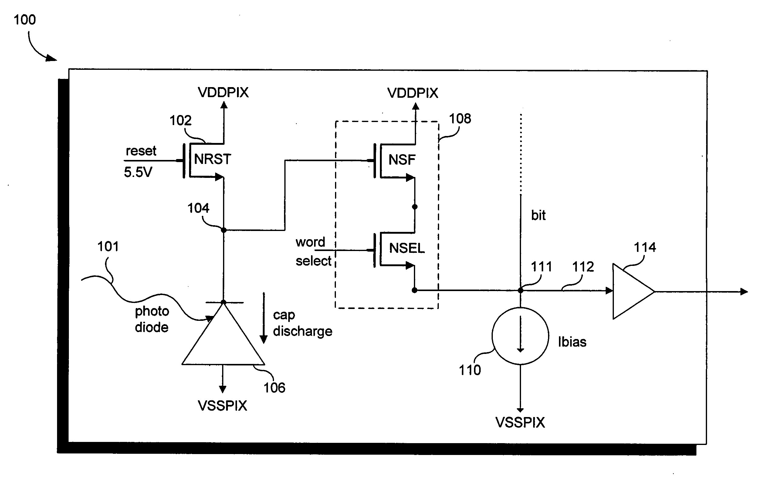
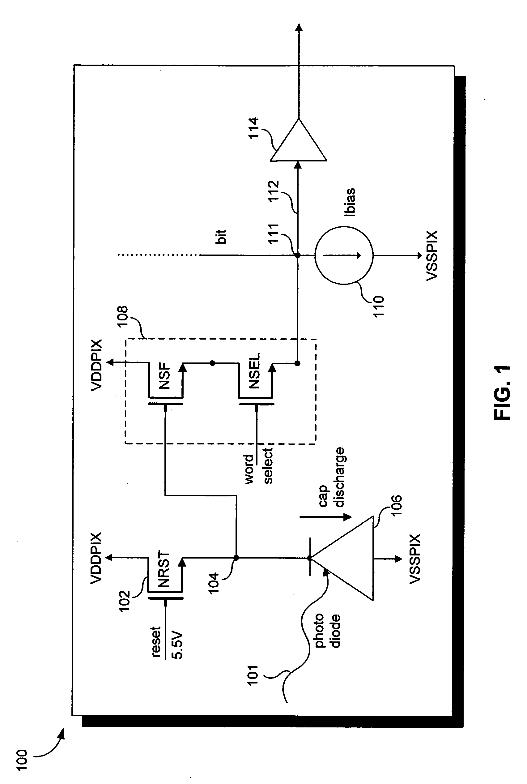
[0034]FIG. 1 illustrates an active pixel sensor 100 that detects optical energy 101 and generates an analog output 112 that is proportional to the optical energy 101. In embodiments, the active pixel sensor 100 can be implemented in a standard CMOS process, without the need for a specialized optical process.

[0035] The active pixel sensor 100 includes a reset FET 102, a photo-diode 106, a source follower 108, a current source 110, an amplifier 114, and an analog-to-digital converter 116. The photo-diode 106 is coupled to the source of the reset FET 102 at a discharge node 104. The drain of the reset FET 102 is coupled to a power supply VDD. The node 104 is also coupled to the gate input of the source follower 108, the output of which is coupled to output node 111.

[0036] During operation, the reset FET 102 is reset so as to charge the nod 104 to VDD. More specifically, the FET 102 is turned-on using the gate input so that the node 104 charges to VDD, after which the FET 104 is cut-o...


PUM


Abstract

The present invention includes an active pixel sensor that detects optical energy and generates an analog output that is proportional to the optical energy. In embodiments, the active pixel sensor can be implemented in a standard CMOS process, without the need for a specialized optical process. The active pixel sensor includes a reset FET, a photo-diode, a source follower, and a current source. The photo-diode is coupled to the source of the reset FET at a discharge node. The drain of the reset FET is couple to a power supply VDD. The discharge node is also coupled to the gate input of the source follower, the output of which is coupled to output node. In embodiments, shallow trench isolation is inserted between the active devices that constitute the photo-diode, the source follower, or the current source, where the shallow trench isolation reduces leakage current between these devices. As a result, dark current is reduced and overall sensitivity is improved. This enables the active pixel sensor to be integrated on a single substrate fabricated with conventional CMOS processing.

Description

CROSS REFERENCE TO RELATED APPLICATIONS [0001] This Application claims the benefit of U.S. Provisional Application No. 60 / 598,894 filed on Aug. 5, 2004, which is incorporated herein by reference in its entirety.BACKGROUND OF THE INVENTION [0002] 1. Field of the Invention [0003] The present invention generally relates to image processing on a semiconductor circuit, for example image processing on single semiconductor substrate that is fabricated using standard CMOS processing, instead specialized image processing material. [0004] 2. Background Art [0005] Conventional digital imaging devices, such as a digital camera or an optical mouse, utilize a photo-diode or an array of photo diodes to capture and record optical energy. The photo-diode converts optical energy to electrical energy (voltage or current) that can later be digitized and further processed. [0006] The sensitivity of the photo-diode is limited by the “dark current” that is generated by the photo-diode. The dark current is...

Claims


Application Information

Patent Timeline
IPC IPC(8): H01L27/00
CPCH04N5/361H04N25/63
Inventor TERZIOGLU, ESINWINOGRAD, GIL
Owner AVAGO TECH WIRELESS IP SINGAPORE PTE
Why Eureka
Try Eureka