Alloyed semiconductor nanocrystals

a technology of semiconductor nanocrystals and alloys, which is applied in the direction of instruments, non-metal conductors, oxide conductors, etc., can solve the problems of wide emission spectrum, unusually difficult to stop the reaction at the right time and/or quickly enough, and not as sensitive or stable as non-isotopic detection systems that utilize luminescent semiconductor quantum

Active Publication Date: 2006-02-09
CRYSTALPLEX CORP
View PDF20 Cites 49 Cited by
  • Summary
  • Abstract
  • Description
  • Claims
  • Application Information

AI Technical Summary

Benefits of technology

[0007] The present invention includes a novel method of synthesizing alloy semiconductor nanocrystals (SCNs) that eliminates the need to closely time and stop the synthesis process to achieve a desired wavelength, bandwidth or both. The present invention will produce alloy SCNs of the formula WYxZ(1-

Problems solved by technology

While these nonisotopic systems solve the problems associated with radioisotopic detection, such as short half-lives of radioisotopes, health hazards and expensive removal of radioactive waste, they are not as sensitive or stable as nonisotopic detection systems that utilize luminescent semiconductor quantum dots.
For two-element nanocrystal synthesis, the emission wavelength is determined solely by size and is selected by stopping crystal growth at precise

Method used


Image

  • Alloyed semiconductor nanocrystals
  • Alloyed semiconductor nanocrystals
  • Alloyed semiconductor nanocrystals

Examples


example 1

Core Synthesis

[0100] Octadecene (4.00 mL) was mixed with oleic acid (200 μL) and added to CdO (0.1 mmol) in a three neck round bottom flask. The flask was flushed with 99.999% nitrogen for 20 minutes and then heated to 300° C. until the solution was clear. Stock solutions of selenium and sulfur were prepared in a glove box under 99.999% nitrogen. Selenium powder (1.00 g) was mixed with tributylphosphine (10.00 mL) and sulfur powder (0.40 g) was mixed with octadecene (20.00 mL). 20 μL selenium precursors were mixed with 1.2 mL sulfur precursors in a 20 mL glass vial, diluted to 2.00 mL with octadecene, and then added to the cadmium precursors via a needle syringe (with injection taking less than one second) and stirred for 60 minutes, or until no change in emission wavelength was observed. This produced cores that fluoresce at 525 nm.

Purification

[0101] The entire core solution was added to a 50 mL conical centrifuge tube and 10 mL of hexanes and 30 mL of butanol were added. The ...

example 9

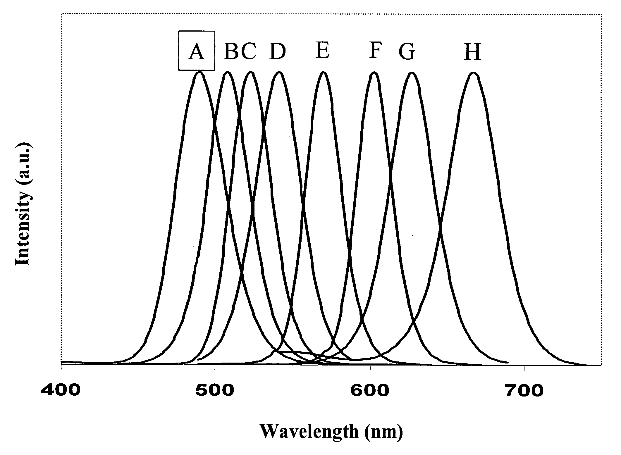
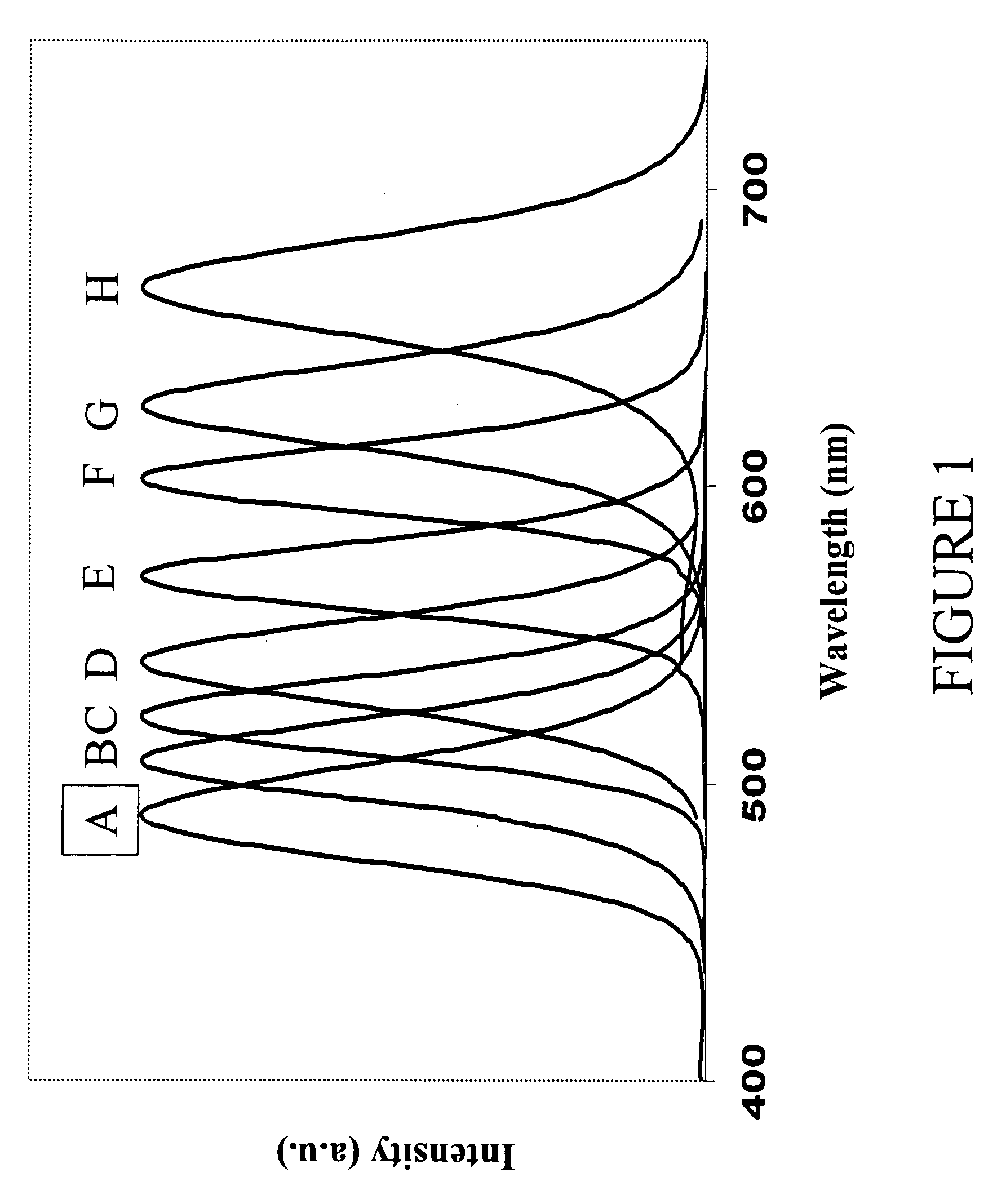
[0103] In a similar way, CdSxSe1-x alloyed semiconductor nanocrystals were prepared using varying ratios of S:Se where the value of x in the resulting CdSxSe1-x alloyed semiconductor nanocrystals ranged from 0.15 to 0.84. FIG. 1 shows the emission spectra of the resulting CdSxSe1-x alloyed semiconductor nanocrystals. The values of x and the resulting wavelengths for samples A through H were as follows: A: x=0.84, wavelength=490 nm; B: x=0.80, wavelength=510 nm; C: x=0.76, wavelength=523 nm; D: x=0.71, wavelength=545 nm; E: x=0.60, wavelength=575 nm; F: x=0.05, wavelength=600 nm; G: x=0.35, wavelength=630 nm; and H: x=0.15, wavelength=665 nm.

[0104] The data from Examples 2-9 can be graphed to provide a calibration curve to determine the proper fraction of selenium and sulfur for the desired wavelength by plotting emission maximum on the X-axis and selenium fraction on the Y-axis.

[0105] The examples have been provided for crystals comprising Cd, Se, and S, but one skilled in the art...

example 10

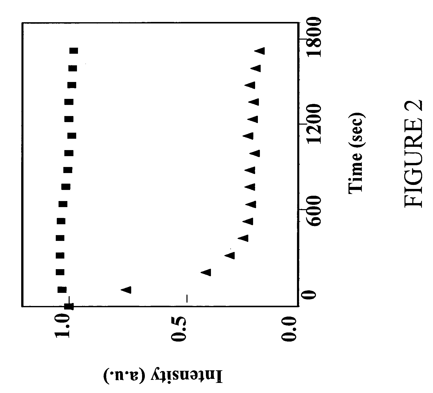
[0106]FIG. 2 provides the results of a photostability comparison of alloyed nanocrystals prepared according to the present invention and nanocrystals made by a conventional method (commercially available). Both nanocrystal samples were illuminated by a UV light source and emission spectra intensities were measured at the indicated time intervals. The two nanocrystal samples have the same emission wavelength at 525 nm. The intensity values were then plotted against the illumination time. Squares (▪) represent nanocrystals prepared according to present invention. Triangles (▴) represent commercially available nanocrystals.


PUM

PropertyMeasurementUnit
Temperatureaaaaaaaaaa
Fractionaaaaaaaaaa

Abstract

The invention relates to methods for preparing 3-element semiconductor nanocrystals of the formula WYxZ(1-x), wherein W is a Group II element, Y and Z are different Group VI elements, and 0<X<1, comprising dissolving a Group II element, a first Group VI element, and a second Group VI element in a one or more solvents. The Group II, VI and VI elements are combined to provide a II:VI:VI SCN precursor solution, which is heated to a temperature sufficient to produce semiconductor nanocrystals of the formula WYxZ(1-x). The solvent used to dissolve the Group II element comprises octadecene and a fatty acid. The solvent used to dissolve the Group VI elements comprises octadecene. The invention also includes semiconductor nanocrystals prepared according to the disclosed methods, as well as methods of using the semiconductor nanocrystals.

Description

[0001] This application claims the benefit of and priority from U.S. provisional application Ser. No. 60 / 598,634, filed Aug. 4, 2004.FIELD OF THE INVENTION [0002] The present invention relates to methods of making alloyed semiconductor nanocrystals, nanocrystals made according to the methods, and methods of using nanocrystals made according to the methods. BACKGROUND OF THE INVENTION [0003] The development of sensitive nonisotopic detection systems for use in biological assays has significantly impacted many research and diagnostic areas, such as DNA sequencing, clinical diagnostic assays, and fundamental cellular and molecular biology protocols. Current nonisotopic detection methods are mainly based on organic reporter molecules that undergo enzyme-linked color changes or are fluorescent, luminescent, or electroactive (Kricka, Ed., Nonisotopic Probing, Blotting, and Sequencing, Academic Press, New York, 1995; Issac, Ed., Protocols for Nucleic Acid Analysis by Nonradioactive Probes,...

Claims


Application Information

Patent Timeline
IPC IPC(8): G11C7/06
CPCB82Y30/00C01B19/007C01P2002/84C01P2004/64C01P2004/84H01L31/0296H01L33/28H01L21/02557H01L21/0256H01L21/02601H01L31/02966H01L31/1832H01L33/0083H01L31/0352
Inventor QU, LIANHUA
Owner CRYSTALPLEX CORP
Why Eureka
Try Eureka