

Method for connecting substrate and composite element
a composite element and substrate technology, applied in the direction of vacuum evaporation coating, chemical vapor deposition coating, lens, etc., can solve the problems of poor optical properties, poor adhesion stability, poor chemical resistance, etc., and achieve the effect of improving the adhesion location and reducing the risk of aging
- Summary
- Abstract
- Description
- Claims
- Application Information
AI Technical Summary
Benefits of technology
Problems solved by technology
Method used
Image

Examples
Embodiment Construction
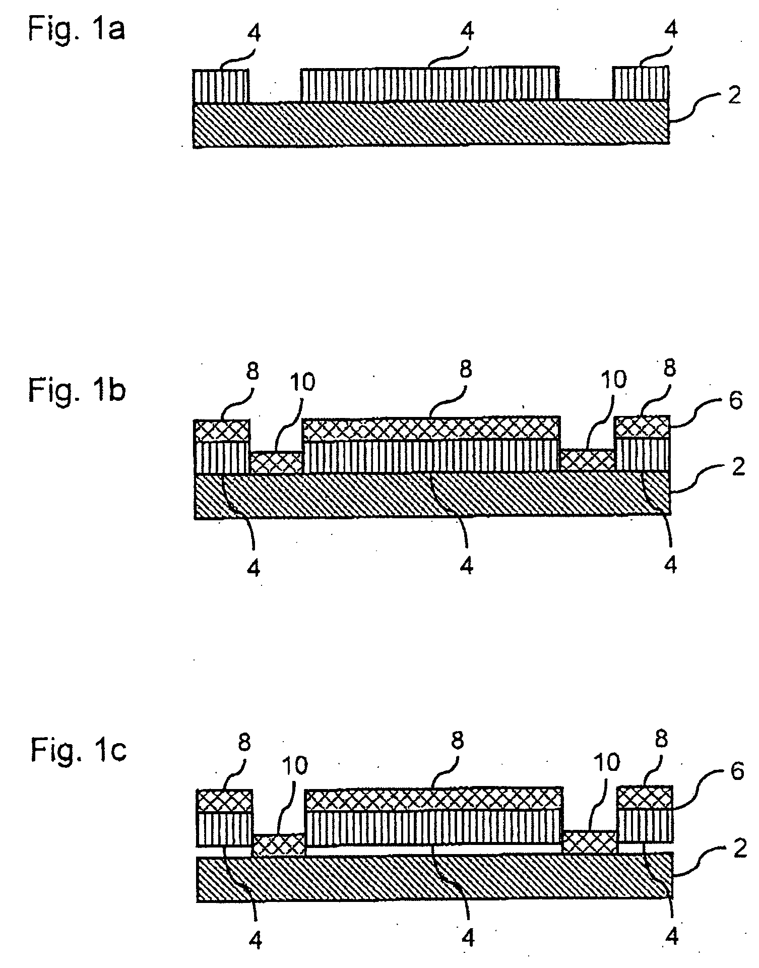
[0091]FIG. 1a shows a substrate 2 made from metal. Alternatively, the substrate 2 may also be a silicon, ceramic or glass substrate. A photoresist 4 has been applied to the substrate 2 using a process known to the person skilled in the art and patterned by photolithography. In this case, the layer of resist represents a mask which adheres securely to the substrate. Alternatively, it is also possible to use a shadow mask or covering mask which does not adhere securely.
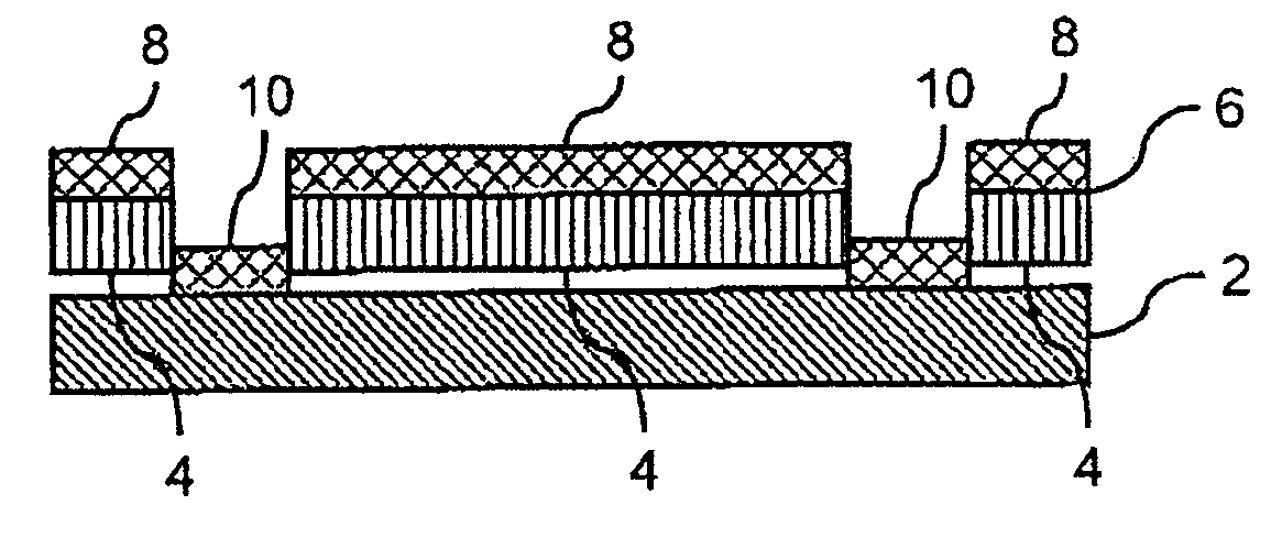
[0092] Then, referring to FIG. 1b, a continuous layer of glass 6 comprising the evaporation-coating glass 8329 is applied by evaporation coating to the substrate 2 and the photoresist 4.
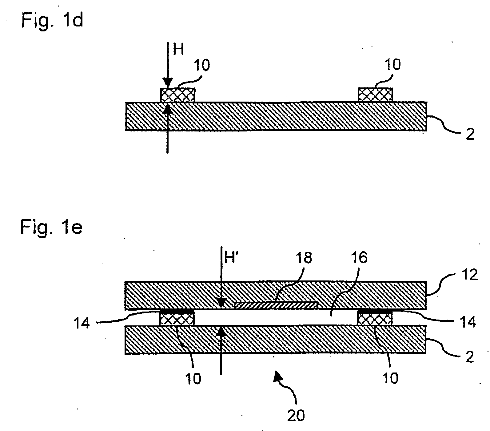
[0093] Referring now to FIG. 1c, the photoresist 4 together with the sections 8 of the glass layer 6 which are present thereon are removed by means of acetone. The sections 10 remain fixedly joined to the metal substrate 2. This process is known as the lift-off process and is one with which the person skilled in the art is familiar.
[0...
PUM
| Property | Measurement | Unit |
|---|---|---|
| temperature | aaaaa | aaaaa |
| thicknesses | aaaaa | aaaaa |
| thicknesses | aaaaa | aaaaa |
Abstract
Description
Claims
Application Information