

Transistor and method of manufacturing the same
a manufacturing method and transistor technology, applied in the direction of basic electric elements, electrical equipment, semiconductor devices, etc., can solve the problems of affecting the performance of the transistor, the damage to the interface between the source/drain region and the substrate, and the failure of the transistor, etc., to achieve excellent electrical characteristics and improve the structure.
- Summary
- Abstract
- Description
- Claims
- Application Information
AI Technical Summary
Benefits of technology
Problems solved by technology
Method used
Image

Examples
embodiment 1
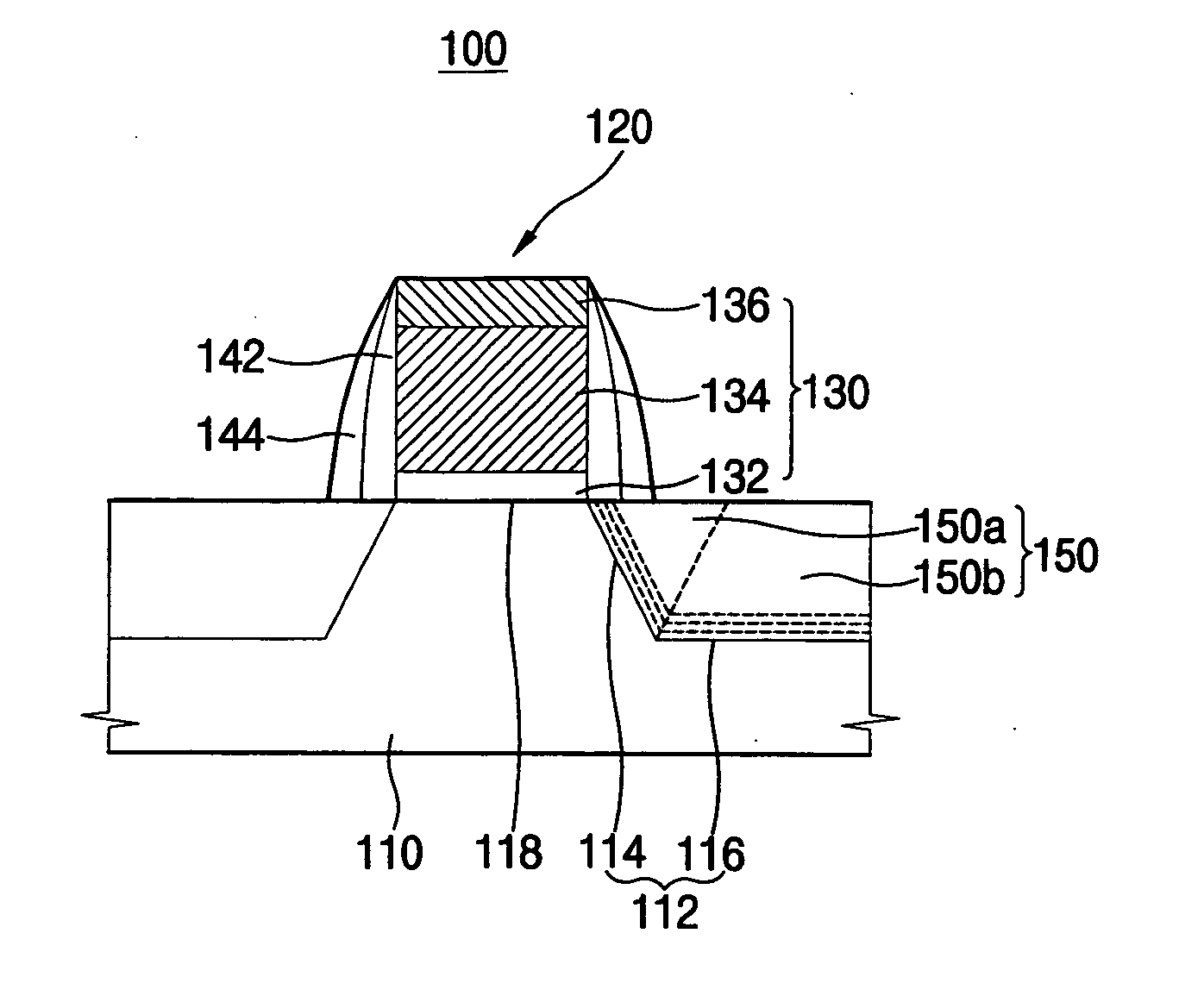
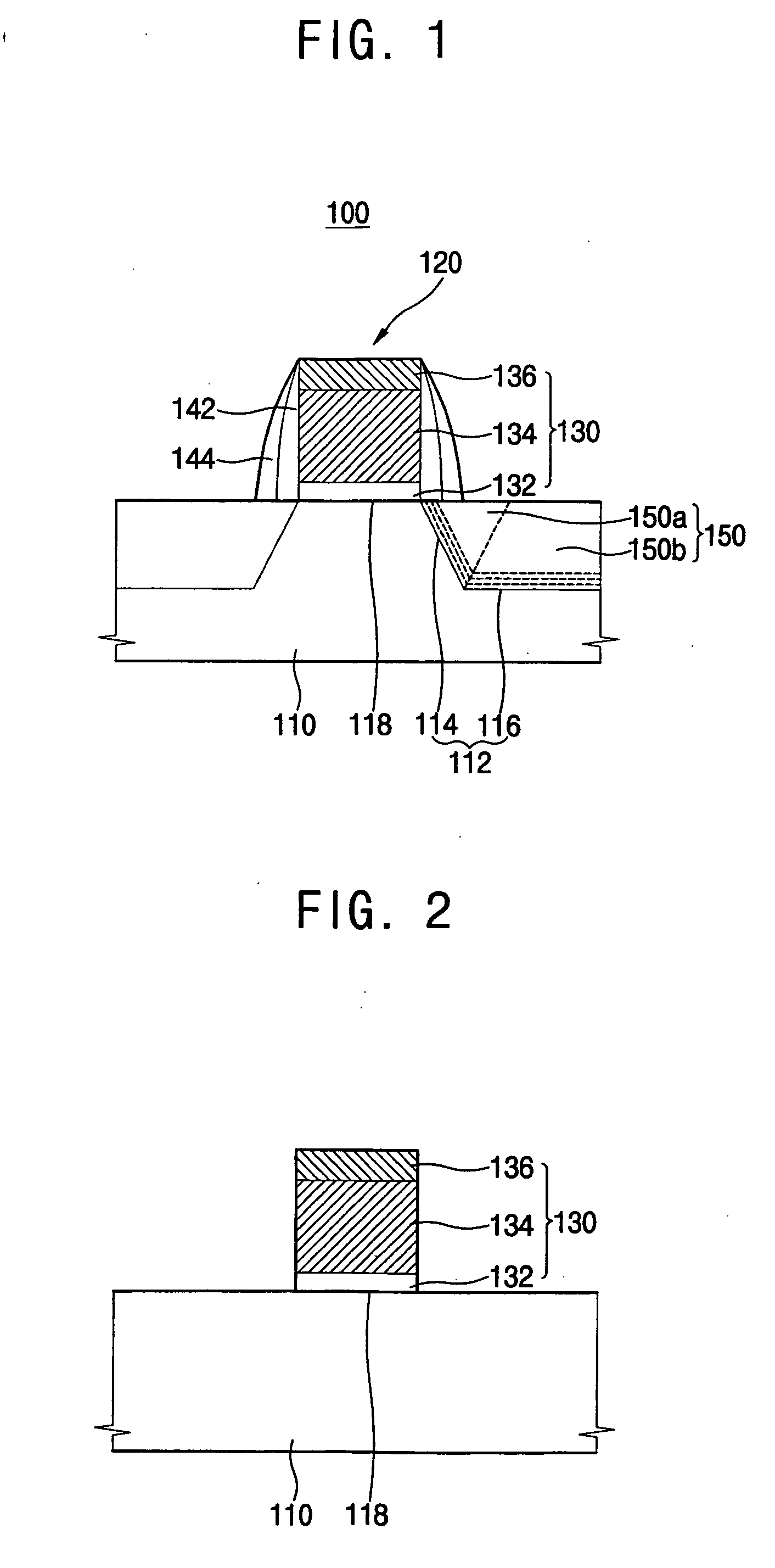
[0063]FIG. 1 is a cross sectional view illustrating a transistor in accordance with a first embodiment of the present invention.
[0064] Referring to FIG. 1, a transistor 100 of the present embodiment includes a semiconductor substrate 110 such as a silicon (Si) substrate or a silicon-germanium (Si—Ge) substrate, a gate structure 120 formed on the semiconductor substrate 110, two epitaxial layers 150 formed at portions of the semiconductor substrate 110 adjacent to the gate structure 120, and impurity regions respectively formed in the epitaxial layers 150.
[0065] The semiconductor substrate 110 has a surface 118 including silicon oriented along the {100} crystal plane. The gate structure 120 is formed on the surface 118 of the substrate 110.
[0066] Two recesses 112 are respectively formed at portions of the surface 118 adjacent to the gate structure 120. The recesses 112 include bottom faces 116 and side faces 114, respectively. The bottom faces 116 include silicon oriented along th...
embodiment 2
[0086] A transistor of a second embodiment of the present invention has elements substantially identical to those of the transistor in FIG. 1 except impurity regions 170 having side faces substantially different from those of epitaxial layers 150 as shown in FIG. 7. The side faces of the impurity regions 170 are respectively positioned between a central portion of a gate pattern 130 and side faces of the epitaxial layers 150. Thus, any further detailed description concerning the transistor of the present embodiment will not be repeated.
[0087]FIGS. 6 and 7 are cross sectional views illustrating a method for manufacturing the transistor in accordance with the present embodiment. In the present embodiment, processes for manufacturing the transistor are substantially identical to those described with reference to FIGS. 2 to 5 except a process for forming the impurity regions 170.
[0088] Referring to FIG. 6, impurities including carbon, boron, phosphorous, etc, are implanted into the ep...
embodiment 3
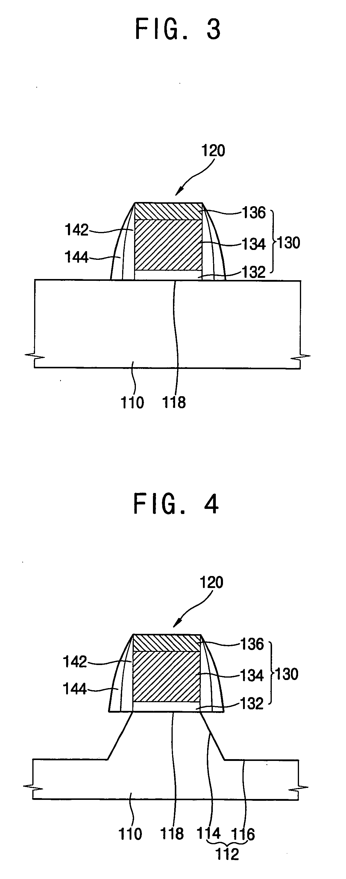
[0091] A transistor of a third embodiment of the present invention has a structure substantially identical to that of the transistor in FIG. 1. Thus, a method of manufacturing the transistor of the present embodiment will be described with reference to FIGS. 8 to 12.
[0092] FIGS. 8 to 12 are cross sectional views illustrating the method of manufacturing the transistor according to the third embodiment of the present invention. In the present embodiment, after first spacers 142 are formed on sidewalls of a gate pattern 130, epitaxial layers 150 are formed in recesses 112 before second spacers 144 are formed on the first spacers 142.
[0093] Referring to FIG. 8, the gate pattern 130 including an insulation layer pattern 132, a conductive layer pattern 134 and a hard mask layer pattern 136 are formed on a surface 118 of a semiconductor substrate 110. The surface 118 includes silicon oriented along the {100} plane.
[0094] Referring to FIG. 9, the first spacers 142 including a nitride are...
PUM
 Abstract
Description
Claims
Application Information