Semiconductor device and method of producing the same

Active Publication Date: 2006-02-23
LAPIS SEMICON CO LTD
View PDF28 Cites 18 Cited by
  • Summary
  • Abstract
  • Description
  • Claims
  • Application Information

AI Technical Summary

Benefits of technology

[0010] In the present invention, the semiconductor is produced with the semiconductor wafer as a single piece in a series of manufacturing steps. Accordingly, it is possible to produce a large number of the semiconductors with radio wave suppression function at a time, thereby reducing production time and improving production efficiency. Further, it is possible to produce the semiconductor device having a size substantially same as a chip size. Accordingly, it is possible to produce a high density conductive pattern substrate with the radio wave suppression function, thereby reducing a size of an electric device.

Problems solved by technology

As a result of the high density, radio interference has become an issue between pins of a semiconductor device or relative to a peripheral device and other semiconductor device.
The radio interference is mainly caused by a radiation noise generated from an active circuit of a semiconductor element.
The radiation noise is generated from a conductive pattern on a mount substrate or a surface of a semiconductor device such as a front surface, a rear surface, or a side surface, thereby causing the radio interference such as radio disturbance and abnormal resonance.
Accordingly, it is necessary to attach the cap in an additional step after the semiconductor device is produced, thereby increasing production time and lowering production efficiency of the semiconductor device.
Accordingly, it is difficult to reduce a chip size to meet the requirement for the high density mounting.

Method used


Image

  • Semiconductor device and method of producing the same
  • Semiconductor device and method of producing the same
  • Semiconductor device and method of producing the same

Examples


first embodiment

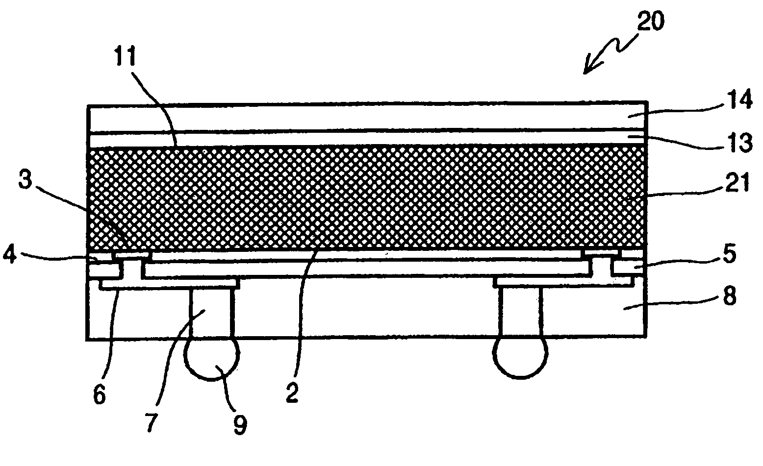
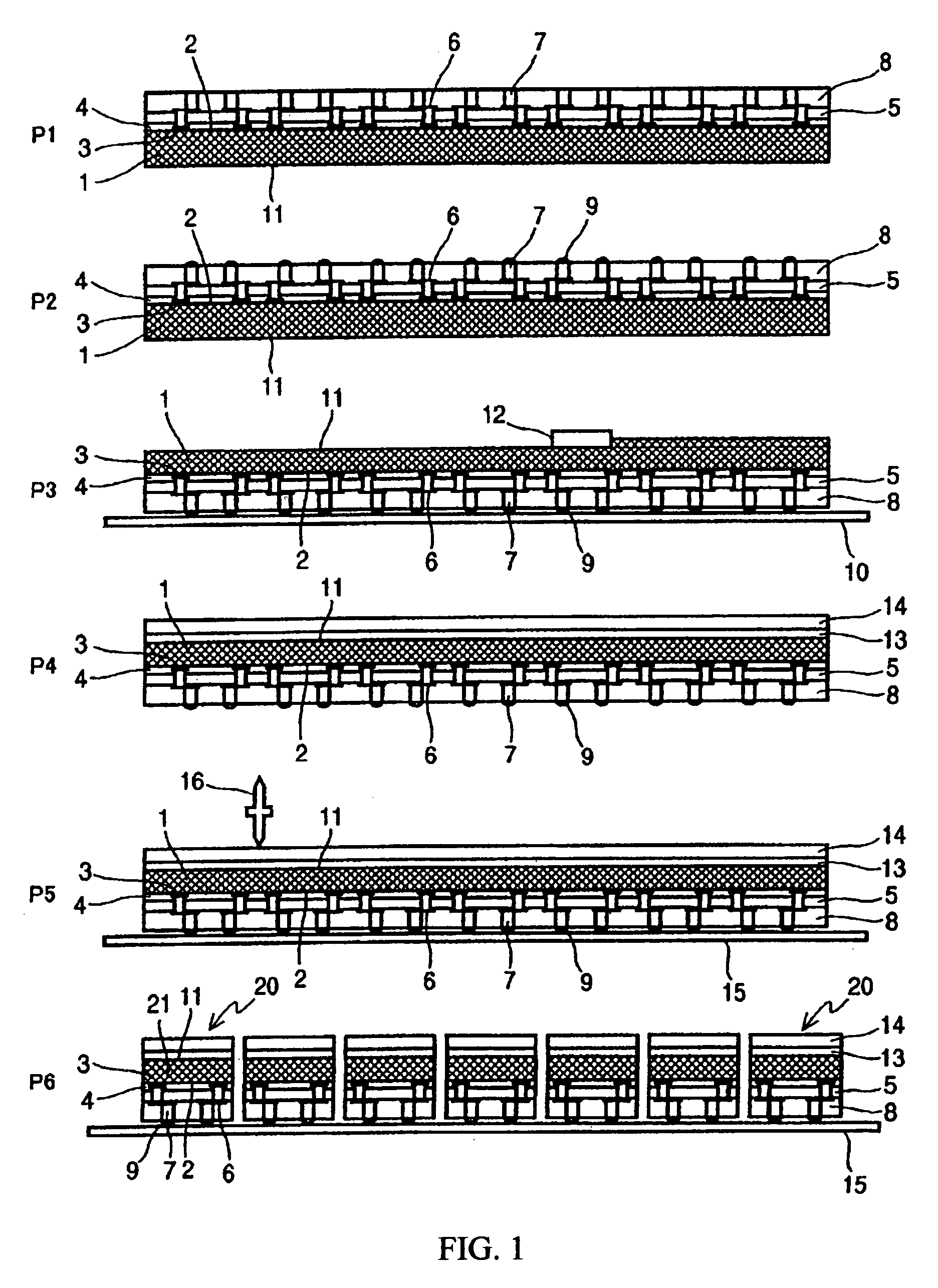
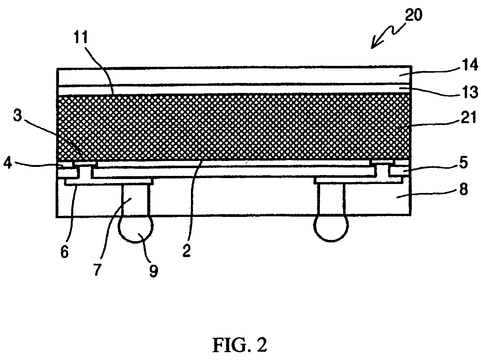
[0024]FIG. 1 is a view showing a method of producing a semiconductor device according to a first embodiment of the present invention. FIG. 2 is a schematic diagram showing the semiconductor device according to the first embodiment of the present invention. In the embodiment, the semiconductor device is a wafer level chip size package type, and a semiconductor wafer 1 formed of silicon and the like is used (shown as a hatched portion in FIG. 1, same in other figures). The semiconductor wafer 1 is provided with a plurality of semiconductor elements such as LSIs formed thereon in advance. On a front surface 2 of the semiconductor substrate 1, there are provided in advance electrodes 3 formed of an aluminum alloy for connecting the semiconductor elements and a protective layer 4 formed of silicon oxide or silicon nitride for protecting active circuits of the semiconductor elements. Holes are formed in the protective layer 4 at locations of the electrodes 3 for connecting re-wirings 6 in...

second embodiment

[0034]FIG. 3 is a view showing a method of producing a semiconductor device according to a second embodiment of the present invention. FIG. 4 is a schematic diagram showing the semiconductor device according to the second embodiment of the present invention. In the second embodiment, components same as those in the first embodiment are designated by the same reference numerals, and explanations thereof are omitted. The semiconductor device is a wafer level chip size package type, and the semiconductor wafer 1 same as that in the first embodiment is used.

[0035] A method of producing the semiconductor device will be explained next as indicated by PA1 to PA6 in FIG. 3. PA1 to PA3 are same as P1 to P3 in the first embodiment, and explanations thereof are omitted. In PA4, after the grinding, the semiconductor wafer 1 is detached from the grind tape 10. A ferrite layer with a specific thickness such as 1 to 5 μm is formed entirely on the backside surface 11 of the semiconductor wafer 1 w...

third embodiment

[0039]FIG. 5 is a view showing a method of producing a semiconductor device according to a third embodiment of the present invention. FIG. 6 is a schematic diagram showing the semiconductor device according to the third embodiment of the present invention. In the third embodiment, components same as those in the first embodiment are designated by the same reference numerals, and explanations thereof are omitted. The semiconductor device is a wafer level chip size package type, and the semiconductor wafer 1 same as that in the first embodiment is used.

[0040] A method of producing the semiconductor device will be explained next as indicated by PB1 to PB6 in FIG. 5. In PB1, the electrodes 3 electrically connected to the active circuits of the semiconductor elements are formed on the front surface 2 of the semiconductor wafer 1 in advance, and a resist layer 30 covers the electrodes 3. Then, a ferrite layer is formed entirely on the front surface 2 of the semiconductor wafer 1 with che...


PUM


Abstract

A semiconductor device of a wafer level chip size package type is formed by cutting a semiconductor wafer with a plurality of semiconductor elements formed thereon in pieces. The semiconductor device includes a semiconductor substrate as the semiconductor wafer having a magnetic layer formed on at least one of a front surface and a backside surface of the semiconductor wafer.

Description

BACKGROUND OF THE INVENTION AND RELATED ART STATEMENT [0001] The present invention relates to a semiconductor device of a wafer level chip size package type, in which a semiconductor wafer with a plurality of semiconductor elements formed thereon is cut in pieces to obtain the semiconductor device. The present invention is also relates to a method of producing the semiconductor device. [0002] An electric device has been developed to have various functionalities processed at a higher speed in a smaller size. With this trend, it has been required to mount electrical elements on a conductive pattern substrate with a higher density. As a result of the high density, radio interference has become an issue between pins of a semiconductor device or relative to a peripheral device and other semiconductor device. [0003] The radio interference is mainly caused by a radiation noise generated from an active circuit of a semiconductor element. The radiation noise is generated from a conductive pa...

Claims


Application Information

Patent Timeline
IPC IPC(8): H01L23/48H01L21/78
CPCH01L23/3114H01L23/552H01L2924/3025H01L2924/01046H01L2924/01078H01L2224/16H01L2224/05569H01L2224/05008H01L2224/05022H01L2224/05001H01L2224/05124H01L2224/05147H01L2924/00014H01L24/05H01L2224/02377H01L2224/05599
Inventor TERUI, MAKOTO
Owner LAPIS SEMICON CO LTD
Why Eureka
Try Eureka