

Film
Inactive Publication Date: 2006-02-23
FUJIFILM CORP +1
View PDF2 Cites 2 Cited by
- Summary
- Abstract
- Description
- Claims
- Application Information
AI Technical Summary
Benefits of technology
[0007] The present invention relates to a film, particularly an insulating film, to solve the above problem, and more specifically
Problems solved by technology
In the field of electronic materials, recently as the integration, multifunctionalization, and performance thereof are advanced, the circuit resistance and the wiring condenser capacity are increased, resulting in increment in power consumption and delay time.
Particularly the increase of the delay time is a great factor for decline of signal speed and occurrence of cross talk in devices, whereby there is demand for reducing the parasitic resistance or parasitic capacity, thereby decreasing the delay time to speed up the devices.
However, when the porosity is increased, the mechanical properties such as elasticity, hardness, and adhesion are significantly deteriorated, peeling of the resultant film, etc. is disadvantageously caused in CMP for forming the copper wirings.
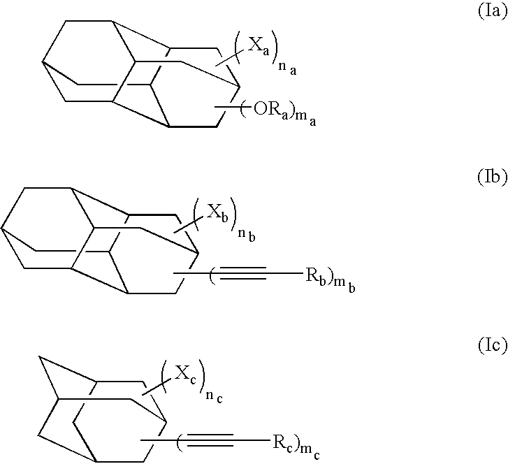
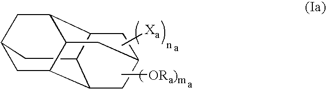
Further, though a method of forming an insulating film comprising polyadamantane ether by chemical vapor deposition is disclosed in JP-A-2003-252982, the ratio of oxygen atoms to total carbon atoms forming the film is high, so that the method has a limitation on lowering the dielectric constant.
Method used
View moreImage
Smart ImageViewing Examples

Examples
example 23
(Example 23)
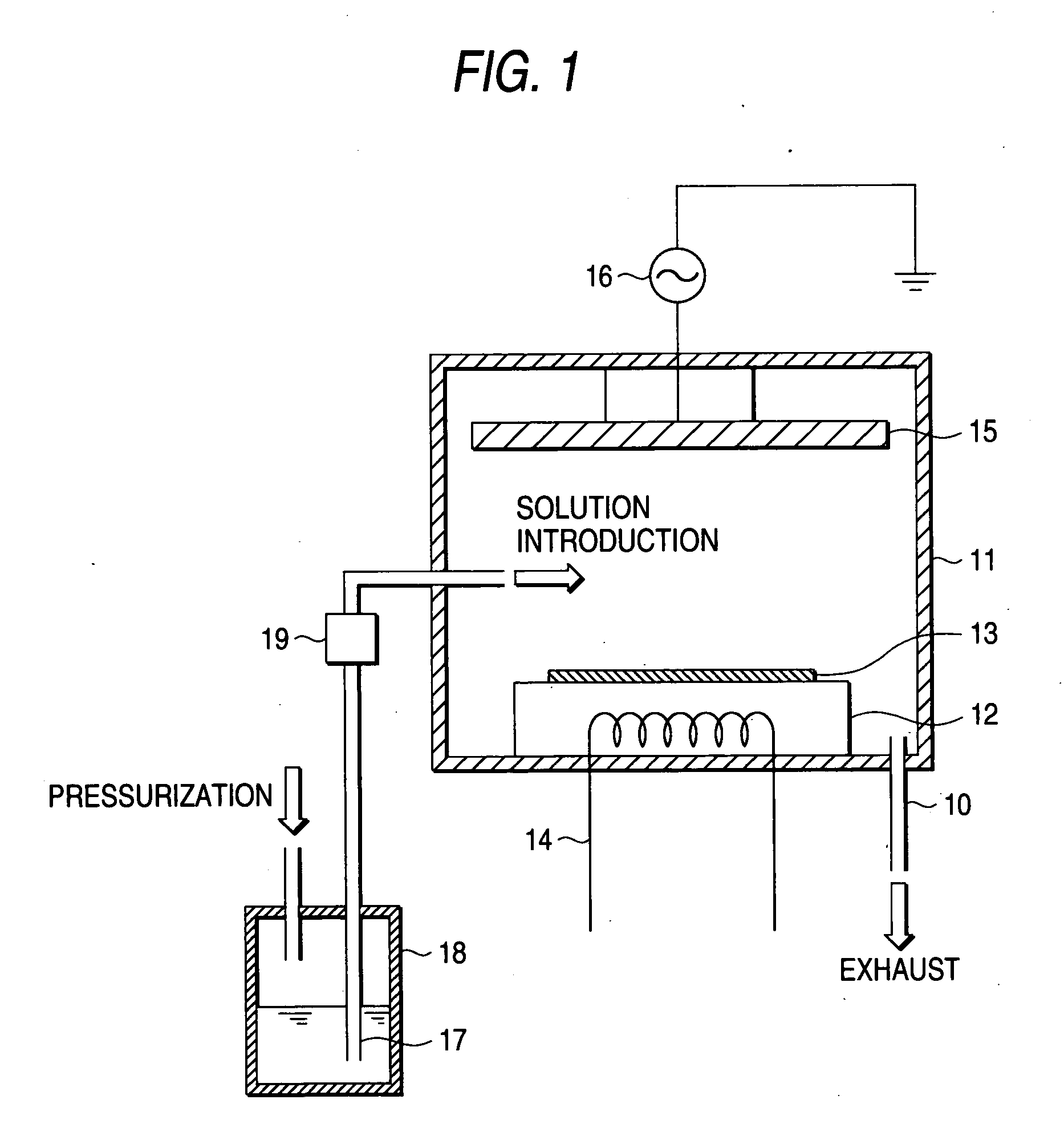
[0082] A high frequency power of e.g. 13.56 MHz was applied at 50 W to the plate-shaped counter electrode 15 while grounding the sample support 12, whereby a film was formed under plasma discharge. The other conditions are the same as in the thermal CVD process. In the case of thus using the plasma CVD process for polymerization, the film formation speed was increased by 1.5 times or more. Further, the films obtained by the process had dielectric constants equal to those of Tables 1 and 2.
[0083] The film of the present invention is a low-dielectric insulating film, and can be used as an interlayer insulating film of electronic devices, etc.
Login to View More PUM
 Abstract
A film formed by chemical vapor deposition of a diamantane or adamantane compound having a particular substituent or a composition containing the compound.
Description
BACKGROUND OF THE INVENTION [0001] 1. Field of the Invention [0002] The present invention relates to a film, and particularly to an insulating film for multilayer interconnection in a semiconductor integrated circuit apparatus. [0003] 2. Description of the Related Art [0004] In the field of electronic materials, recently as the integration, multifunctionalization, and performance thereof are advanced, the circuit resistance and the wiring condenser capacity are increased, resulting in increment in power consumption and delay time. Particularly the increase of the delay time is a great factor for decline of signal speed and occurrence of cross talk in devices, whereby there is demand for reducing the parasitic resistance or parasitic capacity, thereby decreasing the delay time to speed up the devices. Concrete attempts to reduce the parasitic capacity include coating a peripheral part of the wiring with a low-dielectric interlayer insulating film. The interlayer insulating films are ...
Claims
Login to View More Application Information
Patent Timeline
 IPC IPC(8): B32B9/04C23C8/00
CPCB05D1/62H01L21/3121H01L21/312C23C16/30Y10T428/31663H01L21/02118H01L21/02271H01L21/02274H01L21/02126H01L21/02216
InventorWATANABE, KATSUYUKITAN, SHIRO
OwnerFUJIFILM CORP