Integrated circuit and method for establishing transactions

Active Publication Date: 2006-02-23
KONINKLIJKE PHILIPS ELECTRONICS NV +1
View PDF9 Cites 26 Cited by
  • Summary
  • Abstract
  • Description
  • Claims
  • Application Information

AI Technical Summary

Benefits of technology

[0037] Therefore, the utilization of the resources of a network on chip is more efficient, since the connection between modules can be efficiently ad

Problems solved by technology

Systems on silicon show a continuous increase in complexity due to the ever increasing need for implementing new features and improvements of existing functions.
As the number of modules increases however, this way of communication is no longer practical for the following reasons.
On the one hand the large number of modules forms a too high bus load.
On the other hand the bus forms a communication bottleneck as it enables only one device to send data to the bus.
Using networks for on-chip communication when designing systems on chip (SoC), however, raises a number of new issues that must be taken into account.
However, NoC's premises are different from off-chip networks, and, therefore, most of the network design choices must be reevaluated.
On-chip networks have different properties (e.g., tighter link synchronization) and constraints (e.g., higher memory cost) leading to different design choices, which ultimately affect the network services.
Storage (i.e., memory) and computation resources are relatively more expensive, whereas the number of point-to-point links is larger on chip than off chip.
Storage is expensive, because general-purpose on-chip memory, such as RAMs, occupy a large area.
Having the memory distributed in the network components in relatively small sizes is even worse, as the overhead area in the memory then becomes dominant.
For on-chip networks computation too comes at a relatively high cost compared to off-chip networks.
Including a dedicated processor in a network interface is not feasible on chip, as the size of the network interface will become comparable to or larger than the IP to be connected to the network.
Moreover, running the protocol stack on the IP itself may also be not feasible, because often these IPs have one dedicated function only, and do not have the capabilities to run a network protocol stack.
However, data loss also depends on the network architecture, as in most computer networks data is simply dropped if congestion occurs in the network.
Deadlock

Method used


Image

  • Integrated circuit and method for establishing transactions
  • Integrated circuit and method for establishing transactions

Examples


first embodiment

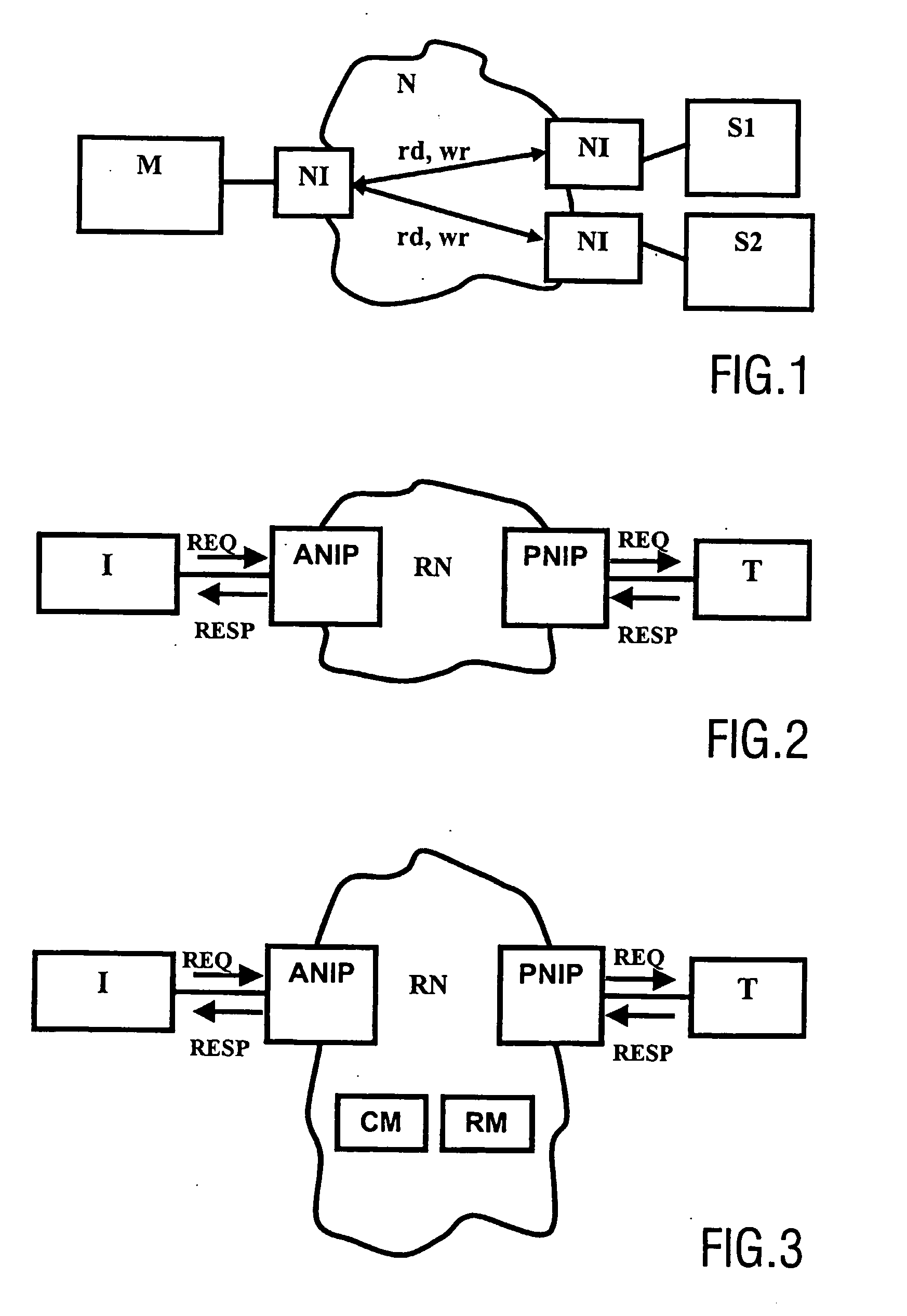
[0051]FIG. 1 shows a System on chip according to a The system comprises a master module M, two slave modules S1, S2. Each module is connected to a network N via a network interface NI, respectively. The network interfaces NI are used as interfaces between the master and slave modules M, S1, S2 and network N. The network interfaces NI are provided to manage the communication of the respective modules and the network N, so that the modules can perform their dedicated operation without having to deal with communication with the network or other modules. The network interfaces NI can send requests such as read rd and write wr between each other over the network.

second embodiment

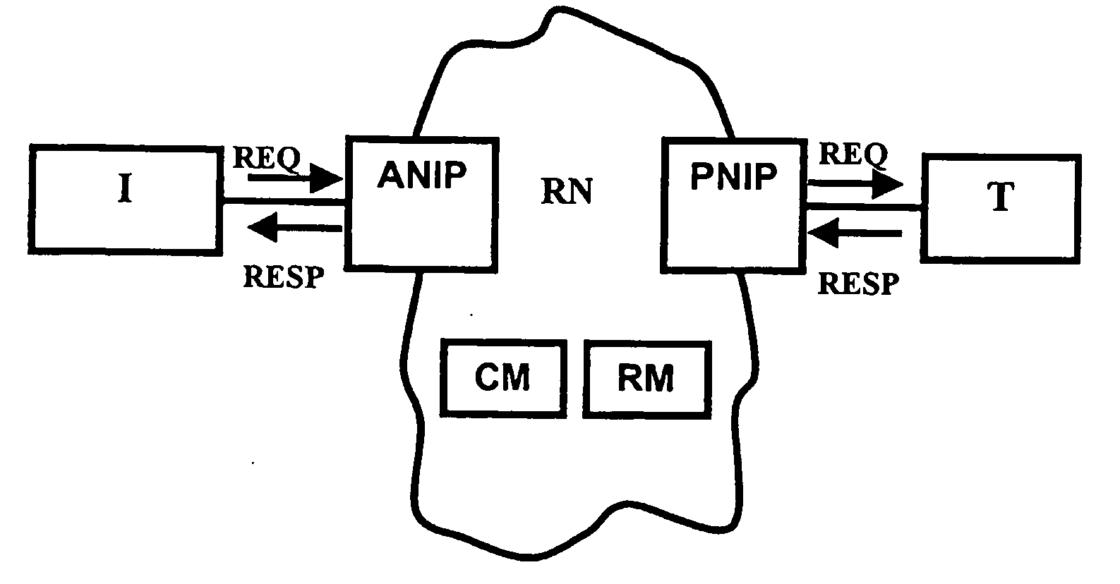
[0052]FIG. 2 shows a system on chip accoding to a The system comprises two modules, namely an initiator I and a target T, a router network RN, and two network interfaces ANIP, PNIP between the modules and the router network RN. The network interfaces provide two network interfaces ports NIP (one request and one response port) through which the modules communicate with the router network RN or other modules via the router network RN. The network interface has one or more ports where modules can be connected. Two different type of ports are available, namely the active network interface port ANIP, which is connected to masters and the passive network interface port PNIP, which is connected to slave. The communication between the initiator module I and the target module T is based on request-response transactions, where the master, i.e. the initiator module L initiates a transaction by placing a request, possibly with some data or required connection properties. The request REQ is del...


PUM


Abstract

An integrated circuit comprising a plurality of processing modules (M; I; S; T) and a network (N; RN) arranged for providing at least one connection between a first and at least one second module is provided. Said connections comprises a set of communication channels each having a set of connection properties. Said connection supports transactions comprising outgoing messages from the first module to the second module and return messages from the second module to the first module. The connection properties of the different communication channels of said connection can be adjusted independently. Therefore, the utilization of the resources of a network on chip is more efficient, since the connection between modules can be efficiently adapted to their actual requirement, such that the connection is not over dimensioned and unused network resources can be assigned to other connections.

Description

FIELD OF THE INVENTION [0001] The invention relates to an integrated circuit having a plurality of processing modules and a network arranged for providing connections between processing modules and a method for exchanging messages in such an integrated circuit. BACKGROUND OF THE INVENTION [0002] Systems on silicon show a continuous increase in complexity due to the ever increasing need for implementing new features and improvements of existing functions. This is enabled by the increasing density with which components can be integrated on an integrated circuit. At the same time the clock speed at which circuits are operated tends to increase too. The higher clock speed in combination with the increased density of components has reduced the area which can operate synchronously within the same clock domain. This has created the need for a modular approach. According to such an approach the processing system comprises a plurality of relatively independent, complex modules. In convention...

Claims


Application Information

Patent Timeline
IPC IPC(8): G06F9/46G06F13/00G06F15/173H04L47/32
CPCH04L47/10H04L49/9073H04L47/32G06F15/173
Inventor RADULESCU, ANDREIGOOSSENS, KEES GERARD WILLEM
Owner KONINKLIJKE PHILIPS ELECTRONICS NV
Why Eureka
Try Eureka