Semiconductor device and method of fabricating a low temperature poly-silicon layer

a low temperature polysilicon and semiconductor technology, applied in semiconductor devices, semiconductor/solid-state device details, electrical apparatus, etc., can solve the problems of grain growth direction that cannot be efficiently controlled, glass substrate deformation, difficulty in etching, etc., to promote the lateral growth of grains, the effect of high practicality

Inactive Publication Date: 2006-03-02
AU OPTRONICS CORP
View PDF8 Cites 195 Cited by
  • Summary
  • Abstract
  • Description
  • Claims
  • Application Information

AI Technical Summary

Benefits of technology

[0011] It is an advantage of the present invention that the semiconductor heat sinks are able to absorb heat from the amorphous silicon layer quickly during the laser crystallization process, thus generating a temperature gradient between the amorphous silicon layer adjacent to the semiconductor heat sinks and other portions of the amorphous silicon layer for promoting the lateral growth of the grains. Particularly, the semiconductor heat sinks can be fabricated using semiconductor materials and apparatuses in a typical LTPS process. Therefore, the present invention does not greatly affect the manufacturing cost and the complexity of the manufacturing process. Consequently, the present invention is highly practical, and is able to completely prevent the problems of the conventional method of fabricating the LTPS layer with metals or insulation materials.
[0012] These and other objects of the present invention will no doubt become obvious to those of ordinary skill in the art after reading the following detailed description of the preferred embodiment that is illustrated in the various figures and drawings.

Problems solved by technology

In the process of fabricating thin film transistor (TFT) liquid crystal displays (LCDs), because the heat resistance of the glass substrate is often under 600° C., and the deposition temperature of the LTPS layer is between 575-650° C., fabricating a poly-silicon layer directly under high temperatures may cause deformation on the glass substrate.
The grain size of the poly-silicon fabricated by typical ELA is about 3000 Å, and the direction of grain growth cannot be efficiently controlled.
However, the film formation of insulation materials, such as aluminum nitride, boron nitride, or diamond like carbon, has to be performed under a high temperature for promoting the thermal conductivity, and there are difficulties in etching while defining the pattern.
Therefore, there are still difficulties in practice.

Method used


Image

  • Semiconductor device and method of fabricating a low temperature poly-silicon layer
  • Semiconductor device and method of fabricating a low temperature poly-silicon layer
  • Semiconductor device and method of fabricating a low temperature poly-silicon layer

Examples


first embodiment

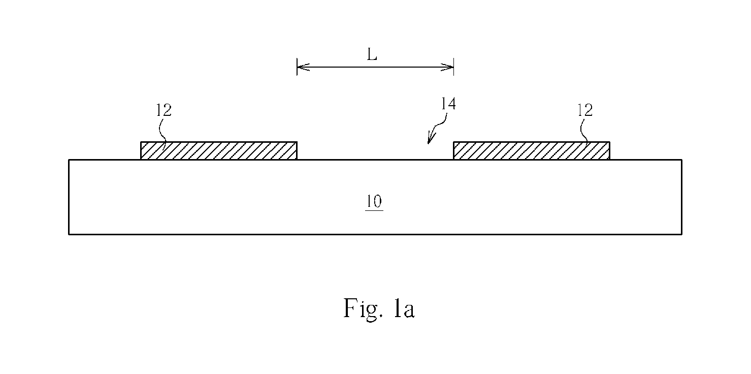
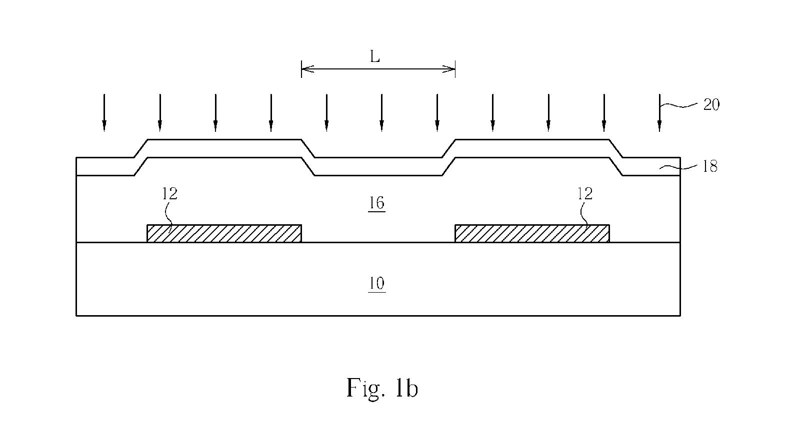
[0019] Please refer to FIGS. 1a-1c. FIGS. 1a-1c are schematic views illustrating a method of fabricating an LTPS layer according to the present invention. As shown in FIG. 1a, the method of the present invention provides a substrate 10, such as a glass substrate, a quartz substrate, or a plastic substrate, and then forms a semiconductor layer (not shown) with a high thermal conductivity over the substrate 10. Following that, portions of the semiconductor layer are removed with a photolithographic and etching process, to generate at least one opening 14 within the semiconductor layer, and to make the remaining semiconductor layer form a plurality of semiconductor heat sinks 12. The opening 14 defines a channel region L, and the semiconductor heat sinks 12 are created around the channel region L. The semiconductor heat sinks 12 are able to absorb thermal energy during a later laser illumination and generate a temperature gradient on an amorphous silicon layer for facilitating the redu...

second embodiment

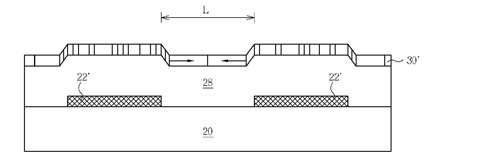
[0022] Please refer to FIGS. 2a-2d. FIGS. 2a-2d are schematic views of a method of fabricating an LTPS layer according to the present invention. As shown in FIG. 2a, the method of the present invention provides a substrate 20, such as a glass substrate, a quartz substrate, or a plastic substrate, and then forms a semiconductor layer (not shown) with a high thermal conductivity over the substrate 20. Following that, portions of the semiconductor layer are removed with a photolithographic and etching process, to generate at least one opening 24 within the semiconductor layer, and to make the remaining semiconductor layer form a plurality of semiconductor heat sinks 22. The opening 24 defines a channel region L, and the semiconductor heat sinks 22 are around the channel region L. The semiconductor heat sinks 22 are able to absorb thermal energy during a later laser illumination and generate a temperature gradient on an amorphous silicon layer for facilitating the reduction of the amoun...


PUM

PropertyMeasurementUnit
temperaturesaaaaaaaaaa
heat resistanceaaaaaaaaaa
adhesiveaaaaaaaaaa

Abstract

A method of fabricating a low temperature poly-silicon (LTPS). A plurality of semiconductor heat sinks are formed over a substrate. A buffer layer and an amorphous silicon layer are formed over the substrate and the semiconductor heat sinks. Following that, a laser crystallization process is performed to transform the amorphous silicon layer into a poly-silicon layer.

Description

BACKGROUND OF INVENTION [0001] 1. Field of the Invention [0002] The present invention is generally related to a semiconductor device and a method of fabricating a low temperature poly-silicon (LTPS) layer, and more particularly, to a semiconductor device and a method of fabricating an LTPS layer using lateral growth. [0003] 2. Description of the Prior Art [0004] In the process of fabricating thin film transistor (TFT) liquid crystal displays (LCDs), because the heat resistance of the glass substrate is often under 600° C., and the deposition temperature of the LTPS layer is between 575-650° C., fabricating a poly-silicon layer directly under high temperatures may cause deformation on the glass substrate. As a result, a method of crystallizing an amorphous silicon layer has been gradually adopted in the present fabrication of LTPS layers of TFT LCDs. [0005] A conventional LTPS layer is fabricated on an insulation substrate, and the insulation substrate must be made of materials pervi...

Claims


Application Information

Patent Timeline
Patent Type & Authority Applications(United States)
IPC IPC(8): H01L29/76H01L23/34H01L29/04
CPCH01L21/2026H01L21/268H01L23/3735H01L23/3738H01L27/1281H01L27/1296H01L2924/0002H01L29/04H01L29/78603H01L2924/00H01L21/02592H01L21/02686H01L21/02422H01L21/02488H01L21/02502H01L21/02532H01L21/02691H01L21/02595H01L21/02667
Inventor CHANG, MAO-YICHEN, YI-WEI
Owner AU OPTRONICS CORP
Why Eureka
Try Eureka