Flash memory device using semiconductor fin and method thereof

a technology of flash memory and semiconductor fin, which is applied in the direction of semiconductor devices, digital storage, instruments, etc., can solve problems such as deteriorating transistor characteristics, and achieve the effect of high scalability, programming or erasing efficiency

Active Publication Date: 2006-03-02
SAMSUNG ELECTRONICS CO LTD
View PDF8 Cites 259 Cited by
  • Summary
  • Abstract
  • Description
  • Claims
  • Application Information

AI Technical Summary

Benefits of technology

[0015] Exemplary embodiments of the present invention provide a flash memory device h

Problems solved by technology

However, as more highly integrated devices continue to be requested in view of high performance, high speed, low

Method used


Image

  • Flash memory device using semiconductor fin and method thereof
  • Flash memory device using semiconductor fin and method thereof
  • Flash memory device using semiconductor fin and method thereof

Examples


Embodiment Construction

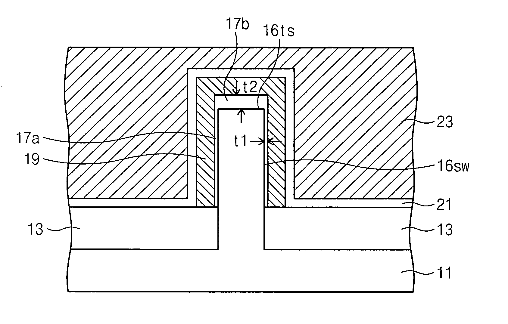
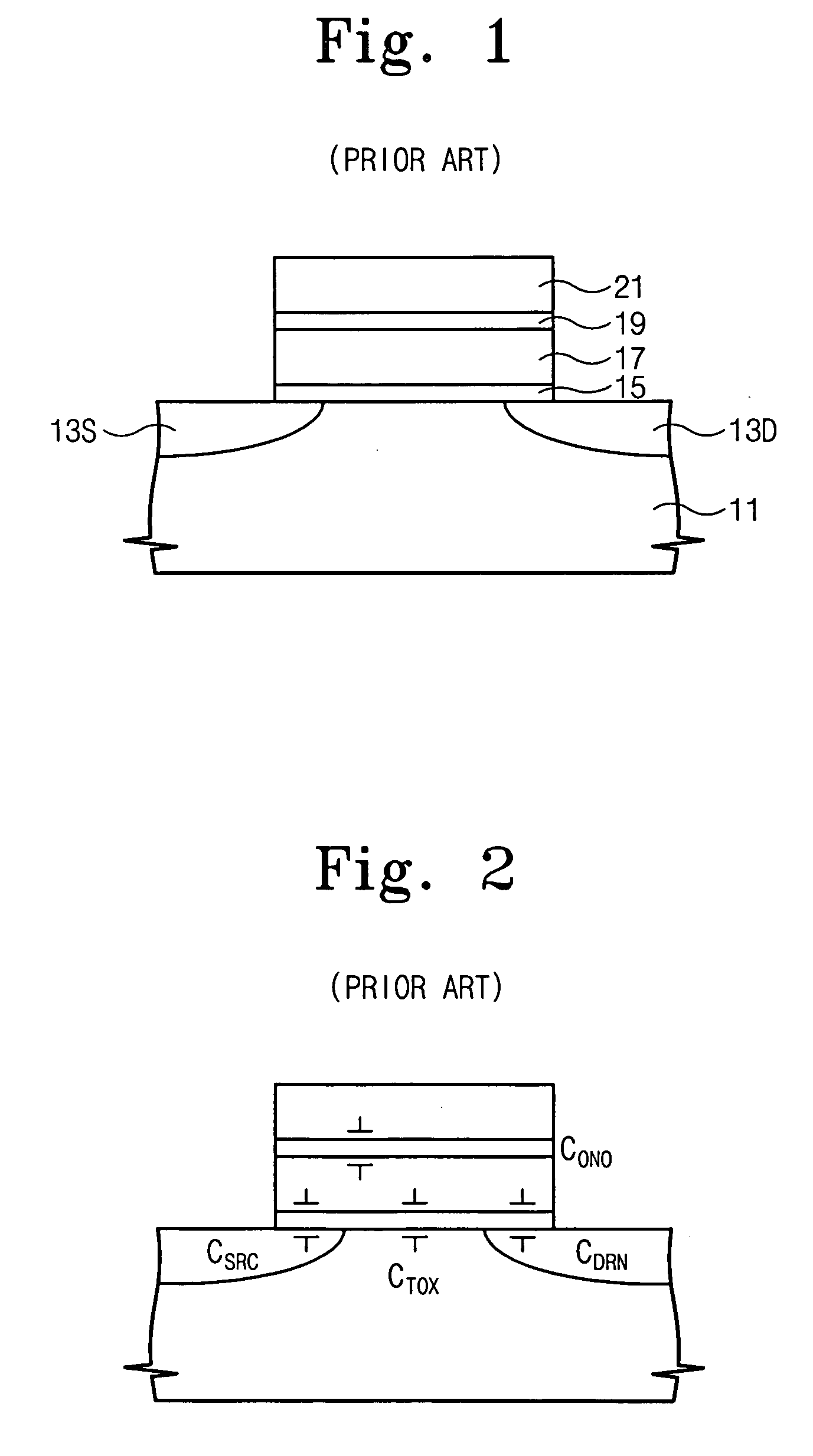
[0049] The present invention will now be described more fully hereinafter with reference to the accompanying drawings, in which preferred embodiments of the invention are shown. This invention may, however, be embodied in different forms and should not be constructed as limited to the embodiments set forth herein. Rather, these embodiments are provided so that this disclosure will be thorough and complete, and will fully convey the scope of the invention to those skilled in the art. It will also be understood that when a layer is referred to as being “on” another layer or substrate, it can be directly on the other layer or substrate or intervening layers may also be present. In the drawings, the thickness of layers and regions are exaggerated for clarity.

[0050] The present invention relates to a flash memory device using a semiconductor fin where an efficiency of a programming and an erase operation is improved and a method thereof. For this, in the present invention, a top surface...


PUM


Abstract

A flash memory device according to the present invention includes a semiconductor fin including a top surface and a side surface originated from different crystal planes. The flash memory device comprises: insulating layers having different thicknesses formed on a side surface and a top surface of the semiconductor fin, a storage electrode, a gate insulating layer and a control gate electrode sequentially formed on the insulating layers. A thin insulating layer enables charges to be injected or emitted through it, and a thick insulating layer increases a coupling ratio. Accordingly, it is possible to increase an efficiency of a programming or an erase operation of a flash memory device.

Description

CROSS-REFERENCE TO RELATED APPLICATIONS [0001] This U.S. non-provisional patent application claims priority under 35 U.S.C. § 119 of Korean Patent Application 2004-69666 filed on Sep. 1, 2004, the entire contents of which are hereby incorporated by reference. BACKGROUND OF THE INVENTION [0002] The present invention relates to a semiconductor device and a method thereof, more particularly, to a semiconductor device using a semiconductor fin and a method thereof. [0003] For the past 30 years, silicon based integrated circuit devices, especially, metal oxide semiconductor MOS devices such as electric field effect transistors FET or MOSFET have been manufactured to have a high speed, a high integration or improved functions, decreasing a cost per a work process, so-called a throughput. However, as more highly integrated devices continue to be requested in view of high performance, high speed, low power consumption and costs, there occur various problems including deteriorating character...

Claims


Application Information

Patent Timeline
IPC IPC(8): G11C7/00
CPCH01L27/11526H01L27/11534H01L29/7881H01L29/66795H01L29/785H01L29/42324H10B41/43H10B41/40H01L21/823437
Inventor PARK, JI-HOONYOON, SEUNG-BEOMHAN, JEONG-UKKIM, SEONG-GYUNKANG, SUNG-TAEGSEO, BO-YOUNGKANG, SANG-WOOPARK, SUNG-WOO
Owner SAMSUNG ELECTRONICS CO LTD
Why Eureka
Try Eureka