Method of manufacturing multi-layered wiring board, electronic device, and electronic apparatus

Active Publication Date: 2006-03-02
SEIKO EPSON CORP
View PDF8 Cites 36 Cited by
  • Summary
  • Abstract
  • Description
  • Claims
  • Application Information

AI Technical Summary

Benefits of technology

[0012] An advantage of the invention is that it provides a method of manufacturing a multi-layered wiring board in which the height of a conductor post can be controlled so as to contribute to improvement of productivity, and electronic devices and electronic apparatuses having a multi-layered wiring board fabricated by the method.
[0013] In order to achieve this, the invention has the following construction.
[0014] A method of manufacturing a multi-layered wiring board is a method of manufacturing a multi-layered wiring board having at least two conductor layers, an interlayer insulation layer provided between the conductor layers, and a conductor post that electrically connects the conductor layers, on a substrate. In the method, the conductor post is formed by repeatedly performing coating a droplet containing a conductive material, applying light energy to the coated droplet, and accumulating and coating a subsequent droplet on the droplet to which the light energy is applied.
[0015] Accordingly, in the manufacturing method of the multi-layered wiring board according to the invention, a droplet containing a coated conductive material can be fixed through dry or baking without spreading the droplet by wetting, by applying lig

Problems solved by technology

In this method, however, pads on which components are mounted cannot be formed in the through hole portion, and the diameter of the through hole is generally about 0.3 mm.
Accordingly, this method is difficult to be used for high-density mounting.
However, since this fabrication method includes a photolithography process or a screen printing process, the process becomes complicated.
The known techniques as described above, however, have the following problems.
As far as the conductor post is concerned, if the conductor post is formed by the droplet discharge

Method used


Image

  • Method of manufacturing multi-layered wiring board, electronic device, and electronic apparatus
  • Method of manufacturing multi-layered wiring board, electronic device, and electronic apparatus
  • Method of manufacturing multi-layered wiring board, electronic device, and electronic apparatus

Examples


Example

First Embodiment

[0046] A droplet coating apparatus applicable to a method of manufacturing a multi-layered wiring board according to the invention will be described first.

[0047] The droplet coating apparatus employs a droplet discharge apparatus (an inkjet device), which is used to discharge droplets through a droplet discharge head and coat a substrate with them.

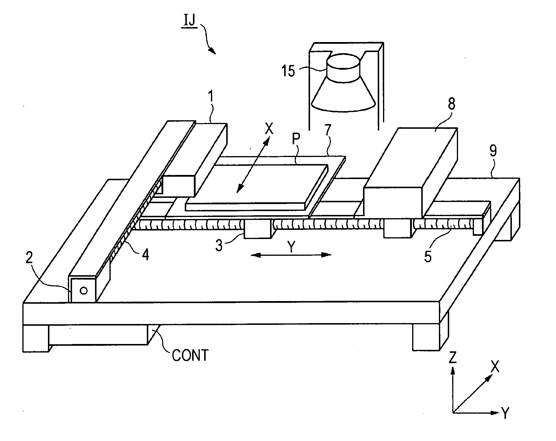
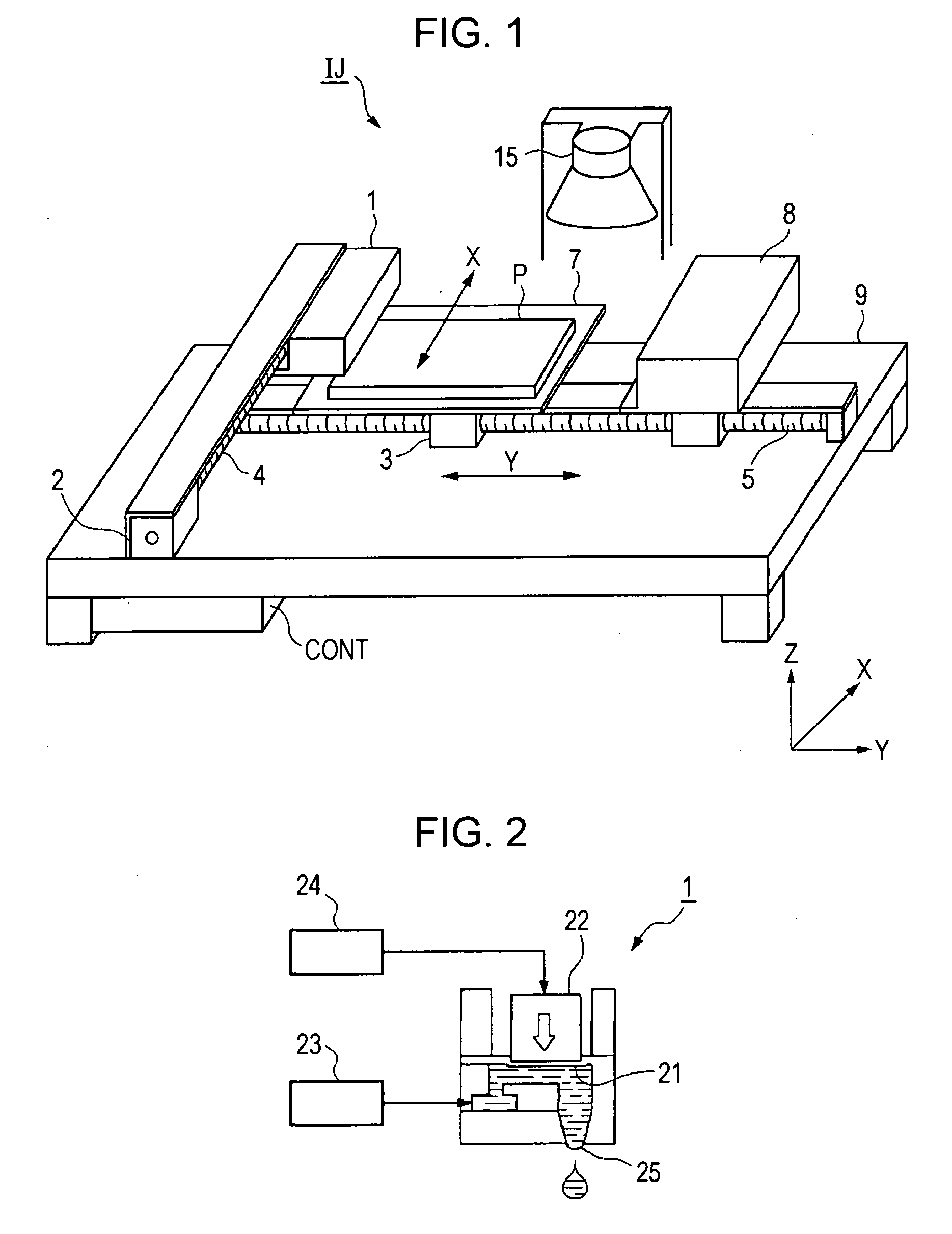
[0048]FIG. 1 is a schematic perspective view showing the construction of a droplet discharge apparatus IJ according to the invention.

[0049] The droplet discharge apparatus (a droplet coating apparatus) IJ includes a droplet discharge head 1, an X-axis-direction driving shaft 4, a Y-axis-direction guide shaft 5, a control device CONT, a stage 7, a cleaning mechanism 8, a base 9, and a heater 15.

[0050] The stage 7 supports a substrate P to which ink (a liquid material) is supplied by the droplet discharge apparatus IJ. The stage 7 includes a fixing mechanism (not shown) that fixes the substrate P to a reference location....

Example

Second Embodiment

[0107] A method of manufacturing a multi-layered wiring board according to a second embodiment of the invention will be described with reference to FIG. 7.

[0108] In the first embodiment, the construction in which the droplet L is coated in a state where the relative motion of the droplet discharge head 1 (the nozzle 25) and the substrate P are stopped has been described. In the embodiment, however, a case where a droplet is discharged, while relatively moving the droplet discharge head 1 (the nozzle 25) and the substrate P with regard to each other (in FIG. 7, the substrate P moves in the right direction) will be described.

[0109] In the embodiment, the nozzles 25 are arranged in a line form in a relative moving direction. The relative moving velocity of the substrate P is synchronized with the discharge frequency of the droplet according to the array pitch between the nozzles. To be more precise, assuming that the array pitch is H, the relative moving velocity of...


PUM

PropertyMeasurementUnit
Energyaaaaaaaaaa
Velocityaaaaaaaaaa
Surface energyaaaaaaaaaa

Abstract

There provided a method of manufacturing a multi-layered wiring board having at least two conductor layers, an interlayer insulation layer provided between the conductor layers, and a conductor post that electrically connects the conductor layers, on a substrate. In the method, the conductor post is formed by repeatedly performing: coating a droplet containing a conductive material, applying light energy to the coated droplet, and accumulating and coating a subsequent droplet on the droplet to which the light energy is applied.

Description

BACKGROUND OF THE INVENTION [0001] 1. Technical Field [0002] The present invention relates to a method of manufacturing a multi-layered wiring board, to an electronic device, and to an electronic apparatus including a multi-layered wiring board manufactured by the above method. [0003] 2. Related Art [0004] Conventionally, a method of manufacturing a multi-layered printed wiring board includes a method implemented by the following processes. [0005] A single-layer substrate on which a pattern is formed by etching is positioned, and then respective layers are laminated thereon. In order to electrically connect upper and lower wiring-line layers, a through hole is formed in a given location of the substrate. By making the circumference of the through hole using plating have conductivity, etc. or by filling the through hole with conductive paste, a multi-layered printed wiring board is formed. [0006] In this method, however, pads on which components are mounted cannot be formed in the th...

Claims


Application Information

Patent Timeline
IPC IPC(8): C23C26/00C23C30/00
CPCC23C4/121C23C26/02H05K3/125H05K2203/1476H05K3/4647H05K3/4664H05K2203/013H05K3/4069C23C4/123H05K3/46
Inventor MIURA, HIROTSUNA
Owner SEIKO EPSON CORP
Why Eureka
Try Eureka