Method for designing an illumination light source, method for designing a mask pattern, method for manufacturing a photomask, method for manufacturing a semiconductor device and a computer program product

a technology of illumination light source and mask pattern, applied in the field of photolithography, can solve the problems of dimensional variation of resist pattern, inability to ensure a sufficient exposure latitude and a sufficient depth of focus for the mask pattern, and difficulty in determining which type of modified illumination is better to us

Inactive Publication Date: 2006-03-02
KK TOSHIBA
View PDF17 Cites 46 Cited by
  • Summary
  • Abstract
  • Description
  • Claims
  • Application Information

AI Technical Summary

Benefits of technology

[0015] A first aspect of the present invention inheres in a computer implemented method for designing an illumination light source, including acquiring a control feature configured to control a dimension of a transferred pattern of a mask pattern; designating a plurality of illumination elements illuminating the mask pattern; designating first illumination lights to each of first polarization states of a light emitted from each of the illumination elements; calculating a first optical image of the control feature, the first optical image formed on a first imaging plane by each of the first illumination lights; and determining an illumination shape and a polarization state distribution of the light, based on an optical characteristic of the first optical image.
[0016] A second aspect of the present invention inheres in a computer implemented method for correcting a mask pattern, including acquiring a control feature configured to control a dimension of a transferred pattern of a mask pattern; designating a plurality of illumination elements illuminating the mask pattern; designating first illumination lights to each of first polarization states of a light emitted from each of the illumination elements; calculating a first optical image of the control feature, the first optical image formed on a first imaging plane by each of the first illumination lights; providing an illumination light source by determining an illumination shape and a polarization state distribution of the light, based on an optical characteristic of the first optical image; and calculating a dimensional variation of the transferred pattern by the illumination light source so as to correct the mask pattern.
[0017] A third aspect of the present invention inheres in a method for manufacturing a photomask, including acquiring a control feature configured to control a dimension of a transferred pattern of a mask pattern; designating a plurality of illumination elements illuminating the mask pattern; designating first illumination lights to each of first polarization states of a light emitted from each of the illumination elements; calculating a first optical image of the control feature, the first optical image formed on a first imaging plane by each of the first illumination lights; providing an illumination light source by determining an illumination shape and a polarization state distribution of t...

Problems solved by technology

Errors induced by the exposure tool may cause a dimensional variation in the resist pattern from a desired value.
For example, the induced errors may include an error of an exposure dose, an error of a height of the substrate with respect to a lens, i.e., a focus error, and the like.
However, when the mask pattern is further miniaturized, even by using the annular illumination or the quadrupole illumination, it may be impossible to ensure a sufficient exp...

Method used


Image

  • Method for designing an illumination light source, method for designing a mask pattern, method for manufacturing a photomask, method for manufacturing a semiconductor device and a computer program product
  • Method for designing an illumination light source, method for designing a mask pattern, method for manufacturing a photomask, method for manufacturing a semiconductor device and a computer program product
  • Method for designing an illumination light source, method for designing a mask pattern, method for manufacturing a photomask, method for manufacturing a semiconductor device and a computer program product

Examples


Embodiment Construction

[0053] Various embodiments of the present invention will be described with reference to the accompanying drawings. It is to be noted that the same or similar reference numerals are applied to the same or similar parts and elements throughout the drawings, and the description of the same or similar parts and elements will be omitted or simplified.

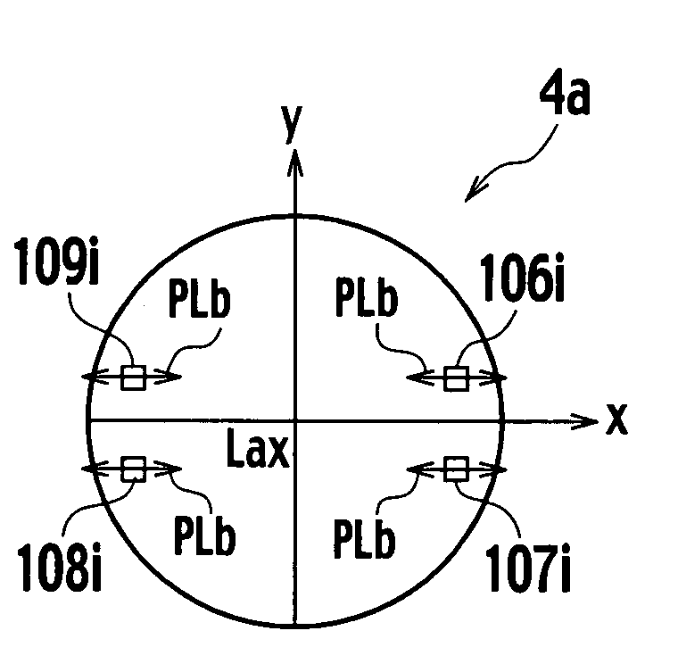
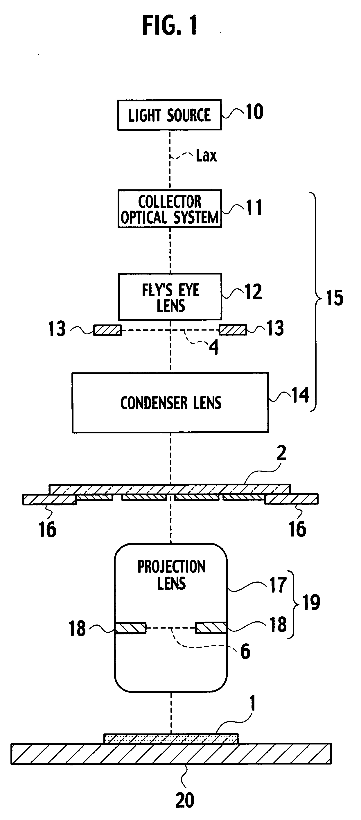
[0054] An exposure tool to be used for description of a method for designing an illumination light source according to an embodiment of the present invention is a refraction type projection reduction exposure tool (scanner), as shown in FIG. 1. A reduction ratio of the scanner is 1 / 4. An argon fluoride (ArF) excimer laser having a wavelength λ of 193 nm is used as a light source 10. An illumination optical system 15 includes a collector optical system 11, a fly's eye lens 12, an illumination aperture 13, a condenser lens 14 and the like. A projection optical system 19 includes a projection lens 17, an aperture stop 18 and the like.

[0055] A...


PUM


Abstract

A method for designing an illumination light source, includes acquiring a control feature to control a dimension of a transferred pattern of a mask pattern; designating a plurality of illumination elements illuminating the mask pattern; designating first illumination lights to each of first polarization states of a light emitted from each of the illumination elements; calculating a first optical image of the control feature, formed on a first imaging plane by each of the first illumination lights; and determining an illumination shape and a polarization state distribution of the light, based on an optical characteristic of the first optical image.

Description

CROSS REFERENCE TO RELATED APPLICATIONS AND INCORPORATION BY REFERENCE [0001] This application is based upon and claims the benefit of priority from prior Japanese Patent Application P2004-243874 filed on Aug. 24, 2004; the entire contents of which are incorporated by reference herein. BACKGROUND OF THE INVENTION [0002] 1. Field of the Invention [0003] The present invention relates to photolithography, and more particularly to a method for designing an illumination light source of an exposure tool, a method for designing a mask pattern, a method for manufacturing a photomask, a method for manufacturing a semiconductor device, and a computer program product for designing an illumination light source. [0004] 2. Description of the Related Art [0005] In an exposure process for manufacturing a semiconductor device, a mask pattern drawn on a photomask is transferred onto a resist film deposited on a semiconductor substrate. In an exposure tool that transfers the mask pattern, a light emit...

Claims


Application Information

Patent Timeline
IPC IPC(8): G03C5/00G03F9/00G06F17/50G03F1/00G03F1/36G03F1/68G03F7/20H01L21/027
CPCG03F7/701G03F7/70566G03F7/705
Inventor FUKUHARA, KAZUYA
Owner KK TOSHIBA
Why Eureka
Try Eureka