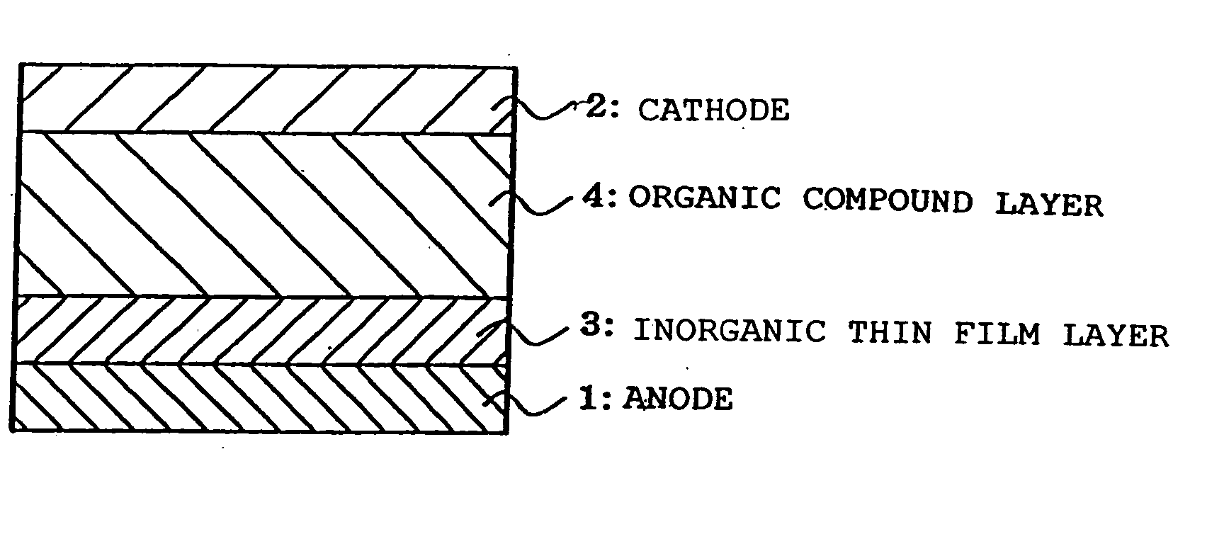
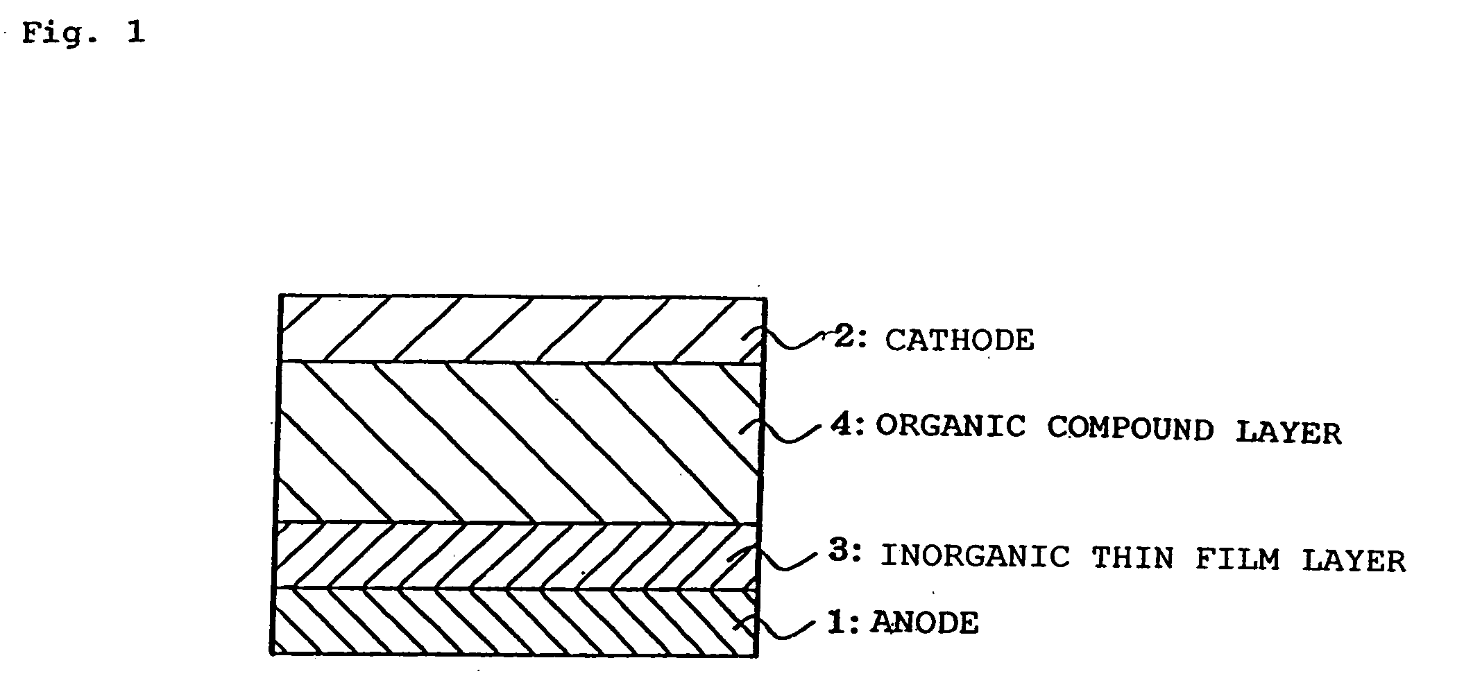
Organic electroluminescence device
- Summary
- Abstract
- Description
- Claims
- Application Information
AI Technical Summary
Benefits of technology
Problems solved by technology
Method used
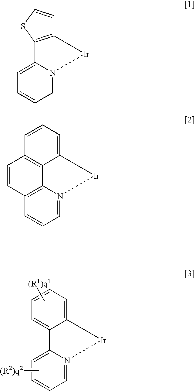
Image

Examples
example 1
[0160] A transparent electrode film, 120 nm thick, made of ITO was formed as an anode layer on a transparent glass substrate 1.1 mm thick, 25 mm long and 75 mm wide. Hereinafter, this combination of the glass substrate and the anode layer is referred to as the substrate.
[0161] Subsequently, this substrate was subjected to ultrasonic washing in isopropyl alcohol, and further dried in a N2 (nitrogen gas) atmosphere. Thereafter, the substrate was washed with UV (ultraviolet rays) and ozone for 10 minutes.
[0162] Next, the substrate was set inside a chamber of a sputtering machine, and further into the chamber was put a target composed of tin oxide and rutheniumoxide (composition: 10 / 1), which would constitute an inorganic thin film layer.
[0163] Furthermore, the inorganic thin film layer was formed in the sputtering machine. The sputtering was performed under the following conditions: a sputtering gas of Ar (30 sccm) and O2 (5 sccm), a substrate temperature of 120° C., a film-forming ...
example 2
[0170] An element was produced in the same way as in Example 1 except that GeO2 was used as the target when the inorganic thin film layer was formed. A pellet of Au having a given size was arranged on this target to film ahigh-resistance inorganic hole injecting layer 7 nm thick.
[0171] The sputtering gas at this time was Ar (30 sccm) and O2 (5 sccm). At room temperature (25° C.), the film-forming rate, the operating pressure and the applying electric power were set to 1 nm / min., 0.2 to 2 Pa, and 500 W, respectively.
example 3
[0172] An element was produced in the same way as in Example 1 except that a target composed of Si oxide and Ir oxide (composition ratio: 10 / 1) was used when the inorganic thin film layer was formed. The inorganic thin film layer was formed into a film thickness of 7 nm.
[0173] The sputtering gas at this time was Ar (30 sccm) and O2 (10 sccm). At room temperature, the film-forming rate, the operating pressure and the applying electric power were set to 1 nm / min., 0.2 to 2 Pa, and 400 W, respectively.
PUM
 Abstract
Description
Claims
Application Information
 - Generate Ideas
- Intellectual Property
- Life Sciences
- Materials
- Tech Scout
- Unparalleled Data Quality
- Higher Quality Content
- 60% Fewer Hallucinations
Browse by: Latest US Patents, China's latest patents, Technical Efficacy Thesaurus, Application Domain, Technology Topic, Popular Technical Reports.
© 2025 PatSnap. All rights reserved.Legal|Privacy policy|Modern Slavery Act Transparency Statement|Sitemap|About US| Contact US: help@patsnap.com