Image forming apparatus

an image forming apparatus and differential output technology, applied in the direction of waveguide type devices, impedence matching networks, pulse techniques, etc., can solve the problems of distorted output waveform, waveform distortion and signal attenuation, and the inability of simple termination resistors to accurately match impedances, etc., to achieve simple configuration

Inactive Publication Date: 2006-03-09
RICOH KK
View PDF4 Cites 18 Cited by
  • Summary
  • Abstract
  • Description
  • Claims
  • Application Information

AI Technical Summary

Benefits of technology

[0050] According to the present invention, it is possible to provide the impedance matching device with a simple configuration capable of controlling an output impedance or an input impedance of a transmitter

Problems solved by technology

Simple termination resistors, however, cannot accurately match the impedances due to a process variation.
As the transmission speed has increased, problems such as waveform distortion and signal attenuation have arisen due to mismatched impedances.
However, with further improvement in transmission speed, if a comparator is connected to an output terminal for monitoring transmission

Method used


Image

  • Image forming apparatus
  • Image forming apparatus
  • Image forming apparatus

Examples


first embodiment

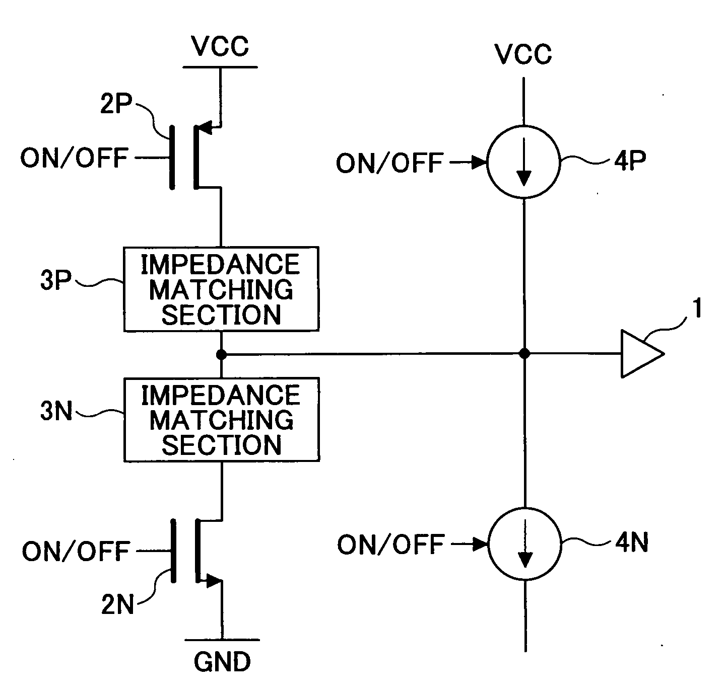
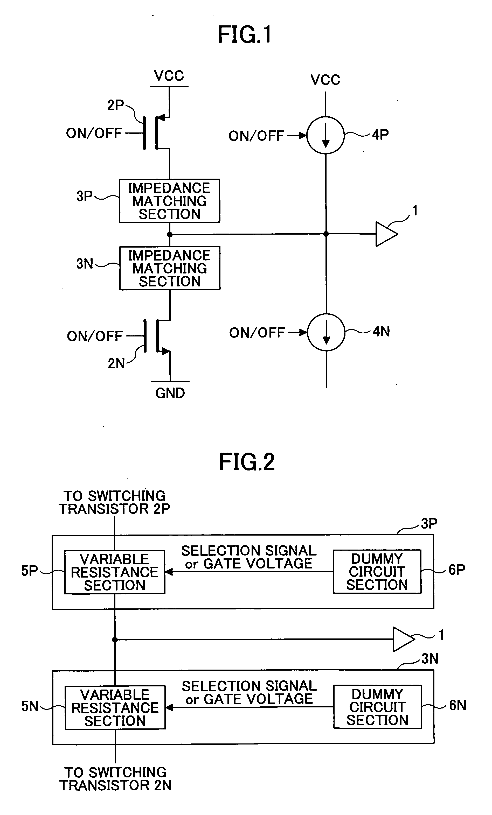
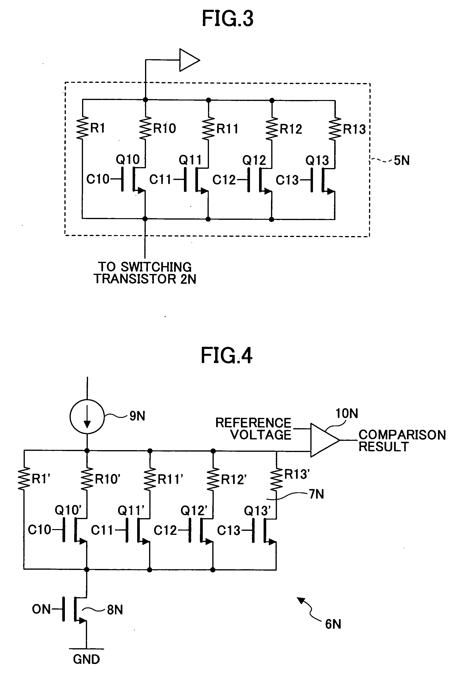
[0079]FIG. 1 is a circuit diagram illustrating a basic configuration example of an output section of an output device applied to high-speed electrical signal transmission according to a first embodiment. The output section of the output device of this embodiment corresponds to, for example, an output section in an integrated circuit (IC chip). An output terminal 1 of the output section is connected to a transmission line (not shown). Roughly, the output section comprises a P-FET switching transistor 2P and a N-FET switching transistor 2N configured to turn on / off according to a predetermined signal so as to switch a data output between “1” (H level) and “0” (L level), a P-type impedance matching section 3P and an N-type impedance matching section 3N configured to adjust and match an output impedance of the output section to a characteristic impedance of the transmission line, and variable current sources (constant current drive sections) 4P and 4N that redundantly output a constant ...

second embodiment

[0117]FIG. 18 is a conceptual diagram illustrating an impedance matching device 103 according to a second embodiment. With reference to FIG. 18, the impedance matching device 103 of this embodiment is provided in an output section or an input section of an integrated circuit 104, and comprises a terminator 101, and a reference voltage generator 102 for controlling the terminator 101. The terminator 101 includes a resistor 105 and a transistor 106 (FIG. 19) as described below. The reference voltage generator 102 generates a reference voltage using an operational amplifier.

[0118]FIG. 19 is a detailed view of the terminator 101 of FIG. 18. As shown in FIG. 19, the terminator 101 includes the resistor 105 and the transistor 106, which are connected in series. The transistor 106 operates within a range of Vds106 can be considered as a variable resistor. It is possible to match a combined resistance of the resistor 105 and the transistor 106 to the characteristic impedance of a transmiss...

third embodiment

[0120]FIG. 21 is a conceptual diagram illustrating an impedance matching device 113 according to a third embodiment. With reference to FIG. 21, an integrator 112 is connected to an output terminal / input terminal. A reference voltage generator 102 controls a terminator 101 by the output voltage of the integrator 112. The integrator 112 calculates the average of the input / output voltage, and the reference voltage generator 102 generates a reference voltage based on the average. Therefore, real-time control suitable for a transmission line and other environments can be performed. According to this embodiment, real-time impedance matching can be achieved with a simple configuration by averaging the output / input voltage.

[0121]FIG. 22 is a circuit diagram of the impedance matching device113 of this embodiment. A resistor 114 and a capacitor 115 connected to the input / output terminal form a lowpass filter, and its voltage is compared to the reference voltage 108. The operational amplifier...


PUM


Abstract

An output device is disclosed that includes an impedance matching section including an impedance adjustment section, and a dummy circuit section having the same configuration as the impedance adjustment section and adapted to calculate an adjustment value for matching an output impedance to a characteristic impedance of the transmission line. The impedance matching section sets the adjustment value to an impedance adjustment section, thereby matching the output impedance to the characteristic impedance. The output device further includes a switching transistor configured to be turned on/off so as to switch the output between an H level and an L level, and a constant current driver configured to add a constant current to the output.

Description

BACKGROUND OF THE INVENTION [0001] 1. Field of the Invention [0002] The present invention relates to an output device, a differential output device, a semiconductor laser modulation drive device, an image forming apparatus, and an electronic device that are applicable to high-speed electrical signal transmission; and particularly relates to an output device and a differential output device that are applicable to high-speed electrical signal transmission and are provided with an impedance matching section for preventing impedance mismatch, which causes signal waveform distortion, between a transmission line and a transmitter in electrical signal transmission between integrated circuits (ICs) or between printed circuit boards (PCBs); and a semiconductor laser modulation drive device, an image forming apparatus, and an electronic device that use these output devices. [0003] The present invention further relates to an impedance matching device for preventing impedance mismatch, which ca...

Claims


Application Information

Patent Timeline
IPC IPC(8): H01P5/12
CPCH03H7/25H03H7/40H04L25/0278H03K19/0005H03H11/30
Inventor OZASA, DANISHIDA, MASAAKINIHEI, YASUHIROOMORI, ATSUFUMI
Owner RICOH KK
Why Eureka
Try Eureka