Enhanced raman amplification and lasing in silicon-based photonic crystals

a technology of photonic crystals and raman, applied in the field of raman microlasers, can solve problems such as cavities in air holes with defects

Inactive Publication Date: 2006-03-09
THE TRUSTEES OF COLUMBIA UNIV IN THE CITY OF NEW YORK
View PDF30 Cites 33 Cited by
  • Summary
  • Abstract
  • Description
  • Claims
  • Application Information

AI Technical Summary

Problems solved by technology

In such embodiments, air-holes with defects can form cavities.

Method used


Image

  • Enhanced raman amplification and lasing in silicon-based photonic crystals
  • Enhanced raman amplification and lasing in silicon-based photonic crystals
  • Enhanced raman amplification and lasing in silicon-based photonic crystals

Examples


Embodiment Construction

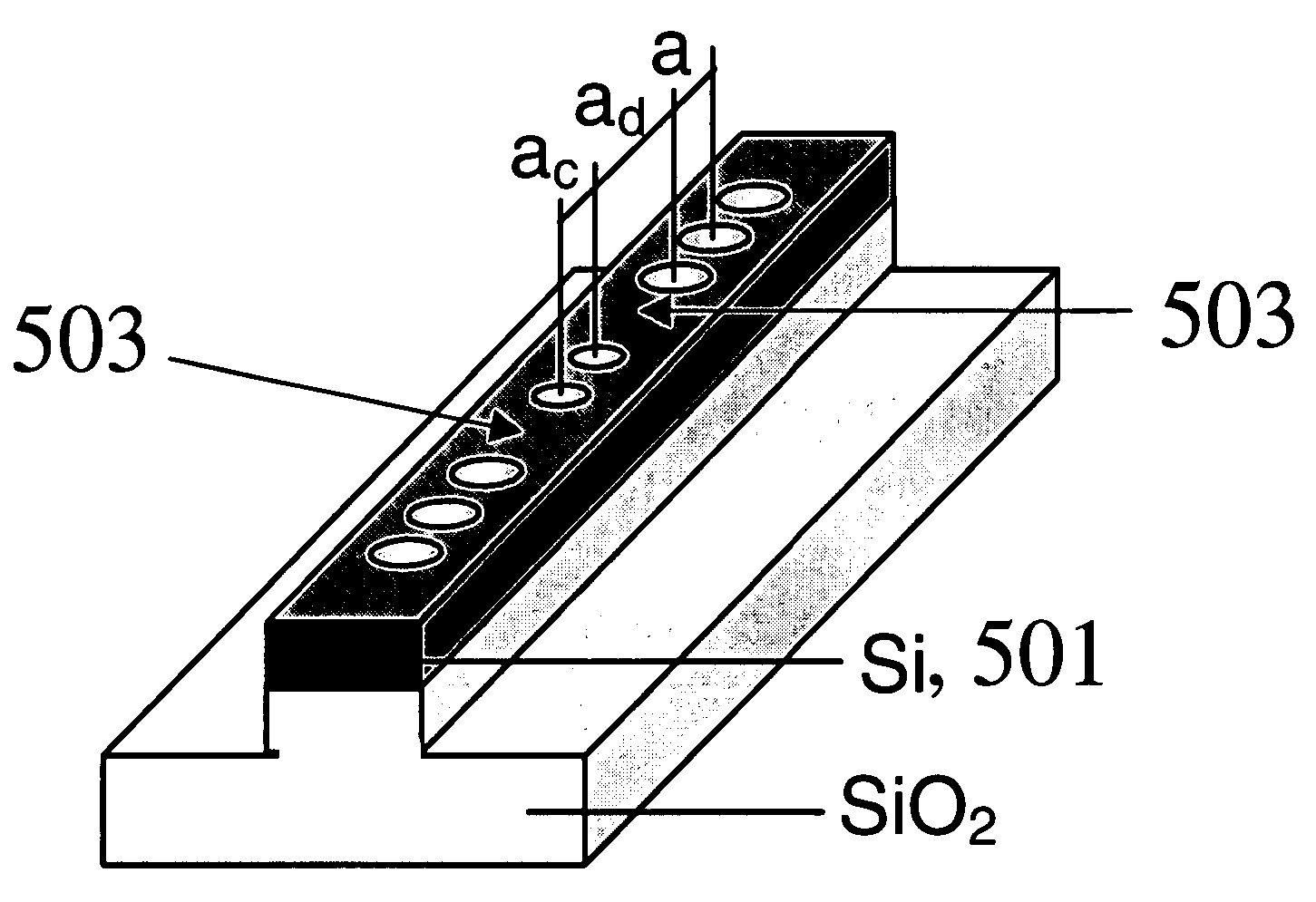
[0033] SRS is a linear inelastic two-photon process, where an incident photon interacts with an excited state of the material. In various embodiments of the present invention, which include the use of photonic crystals made of silicon, the excited state of the material refers to the longitudinal optical (LO) and transversal optical (TO) phonons of crystal silicon. In such embodiments, the strongest Stokes peak arises from single first-order Raman-phonon (threefold degenerate) at the Brillouin zone center of silicon. A microscopic description that depicts the change in the average number of photons ns at the Stokes wavelength ωs with respect to the longitudinal distance z is:  ⅆnsⅆz⁢=(GR-αs)⁢ ⁢ns,GR=(ρi-ρf)1μ1 / 2⁢nsⅆWfiⅆωs,(1)

where GR is the Raman gain, αs an attenuation coefficient, μ the permeability, ⅆWfiⅆωs

the transition rate, and ρi and ρf the initial and final state populations, respectively. For ns and np (the average number of photons at ωp) significantly greater than 1, ...


PUM


Abstract

Tunable laser devices and methods of manufacturing such devices are disclosed. air-holes with defects that form an optical waveguide. The waveguide has a cross-sectional area whose dimensions are in sub-wavelength ranges, wherein the cross-sectional area is perpendicular to the propagation direction of light in the waveguide. The waveguide receives pump light and outputs Stokes light through Raman scattering. The laser device may include a photonic crystal made from silicon having air-holes with defects forming a pair of optically coupled cavities. The geometries of the cavities can be substantially identical to each other. The cavities are defined to cause a frequency-splitting difference between a frequency of pump light and a frequency of Stokes light to correspond to an optical phonon frequency in silicon through Raman scattering.

Description

RELATED APPLICATION [0001] This application claims the priority of U.S. Provisional Application 60 / 589,903 filed on Jul. 20, 2004, which is incorporated herein by reference in its entirety.FIELD OF THE INVENTION [0002] This invention relates to Raman microlasers using photonic crystals made from silicon to achieve low-loss, low-threshold Raman lasing. BACKGROUND OF THE INVENTION [0003] Stimulated Raman scattering (SRS) has a rich and evolving history since the development of the laser. In 1962, Woodbury and Ng discovered the SRS effect at infrared frequencies. [E. J. Woodbury and W. K. Ng, Proc. IRE 50, 2347 (1962)] Hellwarth quickly described this observation as a two-photon process with a full quantum mechanical calculation. [R. W. Hellwarth, Theory of Stimulated Raman Scattering, Phys. Rev. 130, 1850 (1963)] To account for anti-Stokes generation and higher-order Raman effects, however, Garnmire et al. and Bloembergen and Shen then adopted the coupled-wave formalism to describe th...

Claims


Application Information

Patent Timeline
Patent Type & Authority Applications(United States)
IPC IPC(8): H01S3/30H01S5/00
CPCB82Y20/00G02B6/1225H01S3/0635H01S3/0637H01S3/102H01S5/105H01S3/2308H01S3/30H01S3/302H01S3/305H01S5/1021H01S3/1628H01S5/11
Inventor WONG, CHEE WEIYANG, XIADONG
Owner THE TRUSTEES OF COLUMBIA UNIV IN THE CITY OF NEW YORK
Why Eureka
Try Eureka