
Clock buffer circuit

a buffer circuit and clock technology, applied in pulse manipulation, pulse technique, instruments, etc., can solve the problems of clock transmission and other problems, and achieve the effect of improving the reliability of an integrated circuit, simplifying the circuit, and improving the transmission efficiency

Inactive Publication Date: 2006-03-16
RENESAS ELECTRONICS CORP
View PDF14 Cites 14 Cited by
  • Summary
  • Abstract
  • Description
  • Claims
  • Application Information

AI Technical Summary

Benefits of technology

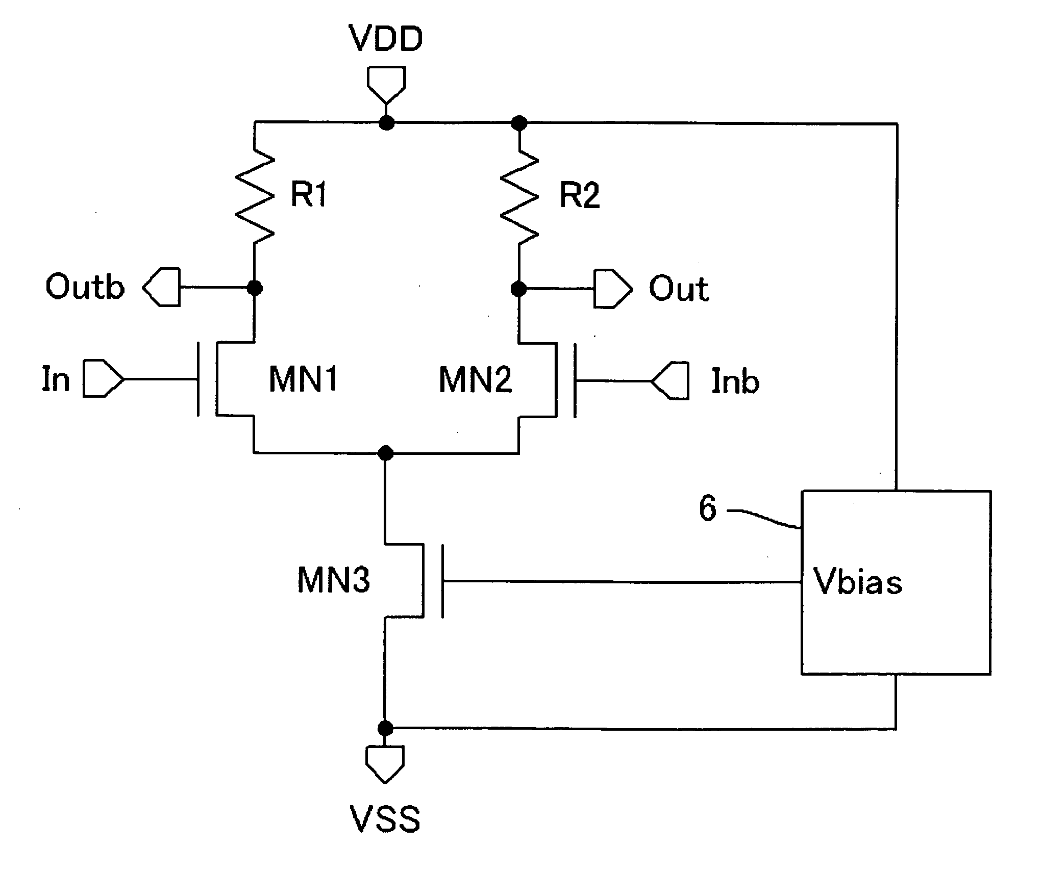
The present invention provides a clock buffer circuit that can cancel out variations in resistance elements and temperature, resulting in a higher speed and lower power consumption. The circuit includes a bias circuit that generates a bias voltage to control the voltage gain of the circuit, and the operating current changes inversely proportional to the resistance value of the load resistors. This allows for a constant voltage gain regardless of the resistance value, and simplifies the circuit design and reduces the required area for circuit integration. The invention also eliminates the need for additional circuits such as offset canceling circuits or direct-current bias circuits, improving transmission efficiency and reliability.

Problems solved by technology

The example of the first technique in Patent Document 1 has various problems associated with the capacitive coupling.
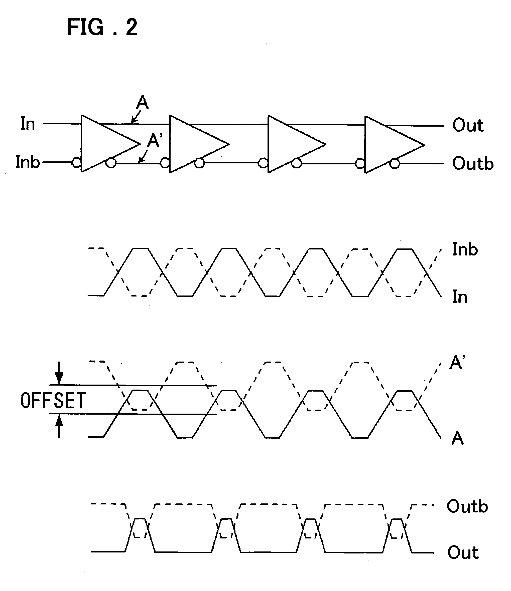
The problem of the example of the second technique in Patent Document 1 is an influence on a transmission speed associated with the direct-current feedback and an influence on the gain of the buffer.
When the gain is set to a lower value, the gain may be lowered at a clock frequency required, so that clock transmission may also be affected.

Method used


Image

  • Clock buffer circuit
  • Clock buffer circuit
  • Clock buffer circuit

Examples


first embodiment

[0031]FIG. 4 is a circuit diagram showing a configuration of the bias circuit 6 in a first embodiment of the present invention. The output of a band-gap reference voltage source 23 is connected to the positive-phase input terminal of an operational amplifier 24. The output of the operational amplifier 24 is connected to the gate electrodes of NMOS transistors MN31 and MN32 for performing voltage-to-current conversion. The source electrodes of the NMOS transistors MN31 and MN32 are respectively connected to one end of an internal resistor25 and one end of an external reference resistor 26 through an external resistance terminal 27. The other ends of the internal resistor 25 and the external reference resistor 26 are connected to the VSS power supply. The internal resistor 25 has the same structure as that of the load resistances R1 and R2 in FIG. 3, and the relative accuracy with respect to the load resistances R1 and R2 is guaranteed. The external reference resistor 26 is the resist...

second embodiment

[0041] The mirror ratio of the current mirror circuit constituted from the PMOS transistors MP36, MP37, and MP38 and the mirror ratio of the current mirror circuit constituted from the PMOS transistors MP39 and MP40 in the first embodiment of the present invention shown in FIG. 4 was set to 1:2 and 1:1, respectively.

[0042] In a certain application circuit, it is sometimes preferable that intermediate setting is performed so that the gain becomes constant and the amplitude is reduced. Now, the current mirror ratio of the PMOS transistors MP36, MP37, and MP38 and the current mirror ratio of the PMOS transistors MP39 and MP40 are 1:2+α and 1:1+α, respectively. The current value of a current Io2 that flows through the drain electrode of the NMOS transistor MP35 becomes as follows, using Equation (8):

Io2=(2+α)*I31−(1+α)*I32   (10)

When the resistance value of the internal resistor 25 is expressed as RINT=REXT*(1+α), Equation (10) is transformed into the following Formula: Io2=(2+α)*V...


PUM


Abstract

Implementing maintenance of a higher speed with fewest possible additional circuits while suppressing deterioration in characteristics of a clock buffer caused by an offset voltage. In a clock buffer circuit comprising a differential amplifier including a pair of load resistances, a pair of differential stage transistors, a constant current source transistor for supplying an operating current to the differential stage transistors, and a bias circuit for supplying to the constant current source transistor a bias voltage according to the resistance value of the load resistances, the bias circuit generates the bias voltage so controlled that the voltage gain of the clock buffer circuit becomes a predetermined value with respect to a variation of the resistance value of the load resistances.

Description

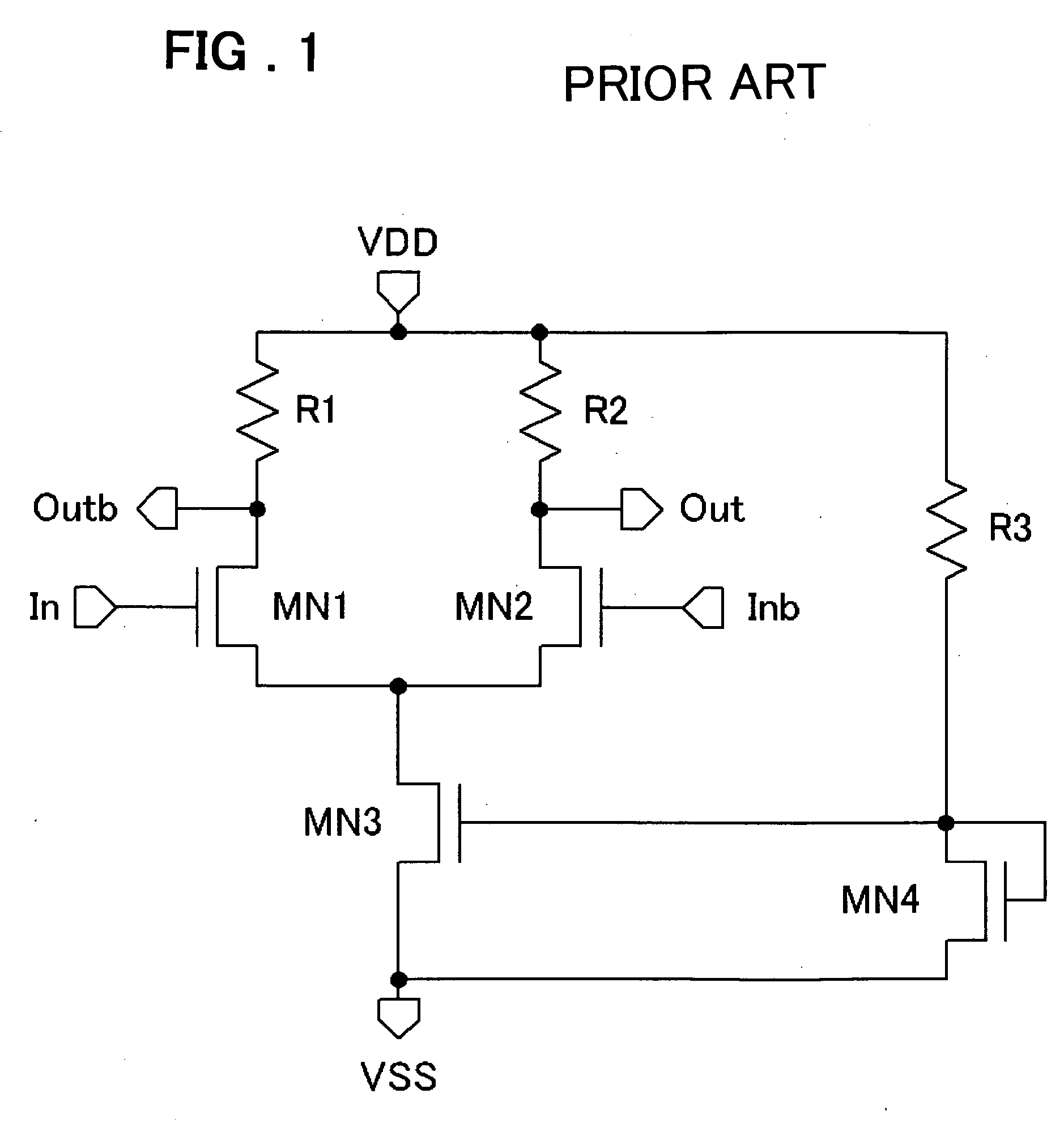
FIELD OF THE INVENTION [0001] The present invention relates to a clock buffer circuit. More specifically, the invention relates to a circuit capable of setting the voltage gain of the clock buffer circuit to be constant with respect to a variation of resistance elements. BACKGROUND OF THE INVENTION [0002] SCL (Source Coupled Logic) circuits are known as a kind of current mode logic circuits capable of performing low-amplitude and high-speed operation. FIG. 1 is a circuit diagram showing the clock buffer circuit that employs a conventional SCL circuit. Referring to FIG. 1, NMOS transistors MN1 and MN2 are transistors that constitute a differential stage. Load resistances R1 and R2 are connected to the drain electrodes of these transistors and a VDD power supply, respectively. An NMOS transistor MN3 is connected between the source electrodes of the NMOS transistors MN1 and MN2 and a VSS power supply. An NMOS transistor MN4 and a resistance R3 constitute a bias current. The drain elect...

Claims


Application Information

Patent Timeline
Patent Type & Authority Applications(United States)
IPC IPC(8): H03K5/08
CPCH03K19/00384H03K19/018578H03K19/018564
Inventor OGASAWARA, KAZUO
Owner RENESAS ELECTRONICS CORP
Learn More