Power module package having excellent heat sink emission capability and method for manufacturing the same

a technology of power module and heat sink, which is applied in the field of semiconductor devices, can solve the problems of complex and costly manufacturing process of power module packages b>10/b>, power circuit chips generate much more heat, and achieve the effect of simple and low cost method of automated manufacturing and excellent heat dissipation ability

Inactive Publication Date: 2006-03-16
FAIRCHILD KOREA SEMICON
View PDF3 Cites 81 Cited by
  • Summary
  • Abstract
  • Description
  • Claims
  • Application Information

AI Technical Summary

Benefits of technology

[0018] The present invention provides a power module package and a manufacturing method thereof, wi

Problems solved by technology

But power circuit chips generate much more heat than the heat generated by integrated circuits or control chips.
As such, the heat sinking ability of the power module package 10 is limited by the lower EMC 2.
Those skilled in the art understand that there is often a tradeoff between the electrical insulating ability of a molding compound and its thermal conductivity.
Accordingly, a manufacturing process of the power module package 10 is complex and costly.
However, the ceramic heat sink 150 has a

Method used


Image

  • Power module package having excellent heat sink emission capability and method for manufacturing the same
  • Power module package having excellent heat sink emission capability and method for manufacturing the same
  • Power module package having excellent heat sink emission capability and method for manufacturing the same

Examples


first embodiment

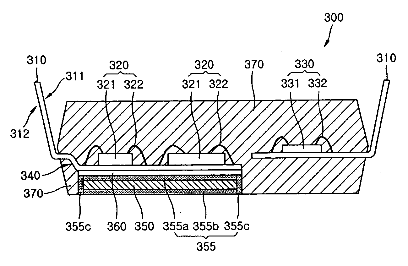
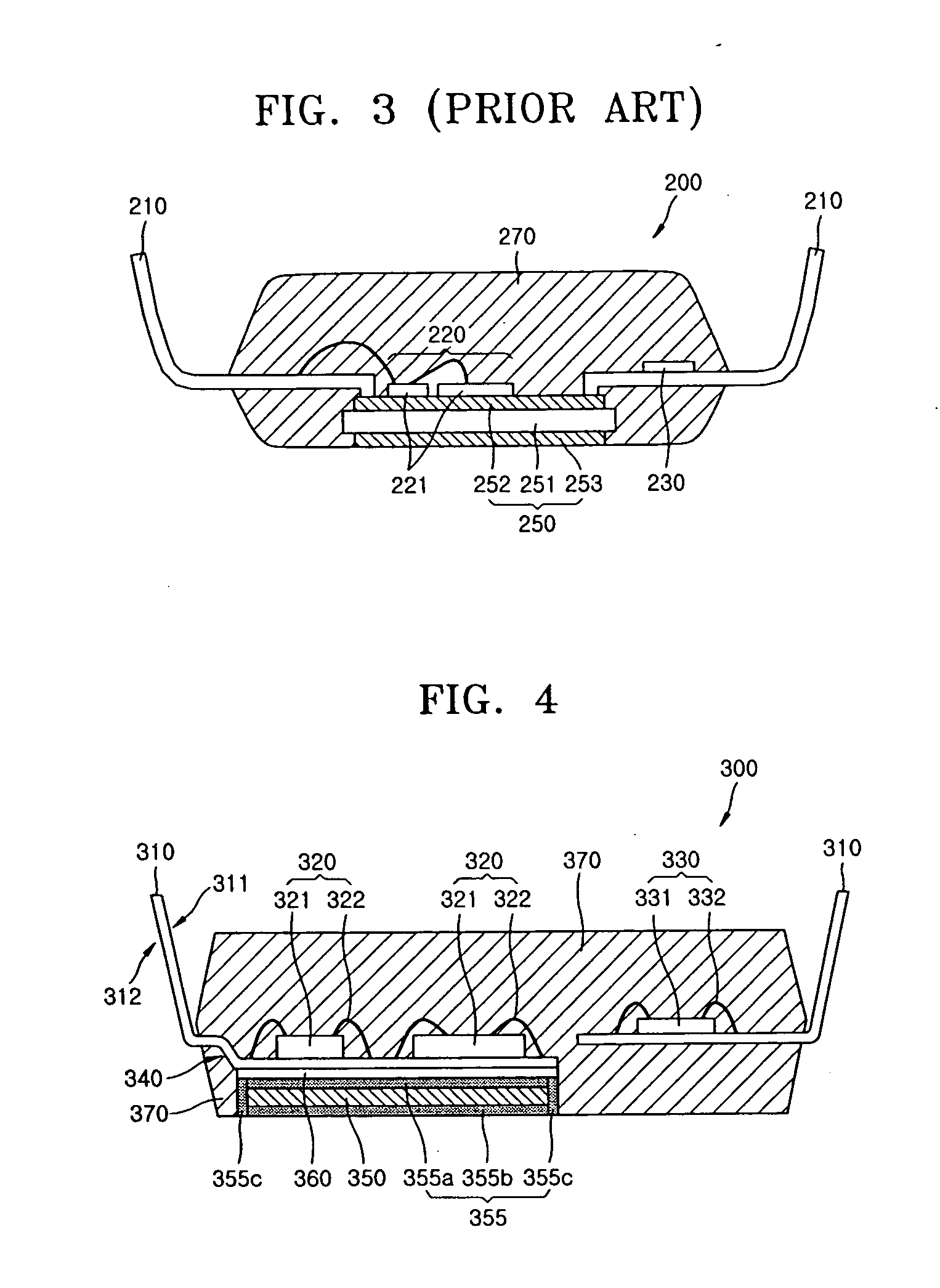
[0041]FIG. 4 is a schematic, cross-sectional view of a power module package according to the present invention.

[0042] Referring to FIG. 4, a power module package 300 includes: a lead frame 310; a power circuit element 320; a control circuit element 330; a metal / metal oxide substrate 350, 355; and an EMC 370.

[0043] The power circuit element 320 includes one or more power circuit chips 321 with aluminum wire 322 to connect the chips 321 to the leads of the lead frame. The aluminum wire 322 has a diameter of about 250-500 μm to endure a high rated current. The control circuit element 330 includes a control circuit chip 331 and a gold wire 332. The aluminum wires 322 and the gold wires 332 properly connect the power circuit chip(s) 321 and the control circuit chip 331, respectively to the leads of the lead frame 310 that extend from inside the package 300 to the outside.

[0044] The lead frame 310 has a thickness of about 0.5-1 mm and has a first surface 311 on which the circuit element...

second embodiment

[0062]FIG. 11 is a flowchart explaining an example of a method for manufacturing a power module package according to the present invention.

[0063] First, aluminum / aluminum oxide substrate 455 is prepared (S21). The aluminum / aluminum oxide substrate 455 includes the heat sink 450 and at least one insulation layer 455a made of the aluminum oxide and formed at least on an upper surface of the heat sink 450. The insulation layer 455a may be formed over an entire surface of the heat sink 450. The aluminum / aluminum oxide substrate 455 may be manufactured by performing a general aluminum oxidation operation known or anodizing. Such anodizing processes are well known.

[0064] The upper wiring layer 452 is directly formed on the insulation layer 455a (S22). The upper wiring layer 452 may be formed on the aluminum oxide layer 455 by a lamination method using Cu, Cu / Ni, Cu / Au, or Cu / Ni / Au, or a sputtering method using the above metal. The upper wiring layer 452 has a properly-shaped wiring patte...

sixth embodiment

[0081]FIG. 9 is a cross-sectional view of one example of a semiconductor package 800 according to the present invention. Referring to FIG. 9, a semiconductor package 800 includes aluminum / aluminum oxide substrate 855, 858, a wiring pattern 852a, external connection pads 852b, a semiconductor element 830, and a sealing resin 870.

[0082] The semiconductor package 800 according to the sixth embodiment is similar in its structure to a flip chip semiconductor package. One difference is that aluminum / aluminum oxide substrate 855, 858 includes an electrical insulation layer 855 made of a plate of aluminum oxide and a plurality of vias 858 made of non-oxidized aluminum that pass through the insulation layer 855. The aluminum / aluminum oxide substrate 855, 858 can be formed by masking an aluminum plate and oxidizing the opposed aluminum to create the vias 858.

[0083] The wiring pattern 852a connected with one end of the vias 858 is formed on a first surface of the aluminum / aluminum oxide subst...


PUM

PropertyMeasurementUnit
Adhesivityaaaaaaaaaa
Electric propertiesaaaaaaaaaa
Thermal conductivityaaaaaaaaaa

Abstract

A power module package includes a power circuit element, a control circuit element, a lead frame, an aluminum oxide substrate having a heat sink and an insulation layer, and a sealing resin. The control circuit element is electrically connected with the power circuit element to control chips within the power circuit element. The lead frame has external connection terminal leads in its edge and has a first surface to which the power circuit element and the control circuit element are attached and a second surface which is used as a heat transmission path. The heat sink is a plate made of metal such as aluminum and the electrical insulation layer is formed at least on an upper surface of the heat sink and made of aluminum oxide. The electrical insulation layer may be formed over an entire surface of the heat sink. Here, the insulation layer is attached to the second surface by an adhesive, on a region below where the power circuit element is attached, to the first surface of the lead frame. In addition, the sealing resin encloses the power circuit element and the control circuit element, the lead frame, and the metal oxide substrate and exposes the external connection terminals of the lead frame.

Description

CROSS-REFERENCE TO RELATED APPLICATIONS [0001] This application claims the priority of Korean Patent Application No. 2004-66176, filed on Aug. 21, 2004, in the Korean Intellectual Property Office, the disclosure of which is incorporated herein in its entirety by reference. BACKGROUND OF THE INVENTION [0002] 1. Field of the Invention [0003] The present invention relates to a semiconductor package, and more particularly, to a power module package having excellent heat transfer characteristics. [0004] 2. Description of the Related Art [0005] Generally, a semiconductor package is manufactured in the following way: one or more semiconductor chips, such as power semiconductor devices or integrated circuits, are mounted on a lead frame or a printed circuit board (PCB), then sealed with an epoxy molding compound (EMC) for protecting the chips, and the packaged chips are mounted on a mother board or a PCB for a system. As used hereinafter the word “chip” means a semiconductor power device or...

Claims


Application Information

Patent Timeline
IPC IPC(8): H02M1/00
CPCH01L23/4334H01L23/49575H01L2924/1305H01L2924/13055H01L2224/48137H01L2224/45144H01L2224/45124H01L2924/01019H01L24/48H01L2924/01079H01L2924/01078H01L25/162H01L25/165H01L2224/48091H01L2224/48247H01L2924/01004H01L2924/00014H01L2924/00H01L2224/45015H01L24/45H01L2924/14C04B37/028C04B2237/343C04B2237/402H01L2924/181H01L2924/2076H01L2924/00015H01L2224/05599H01L2924/00012H01L23/34
Inventor LEE, JOOSANGJEON, OSEOBLEE, KEUNHYUKLIM, SEUNGWON
Owner FAIRCHILD KOREA SEMICON
Why Eureka
Try Eureka