Semiconductor element heat dissipating member, semiconductor device using same and manufacturing same

a technology of semiconductor devices and heat dissipating components, which is applied in the direction of semiconductor devices, semiconductor/solid-state device details, electrical apparatus, etc., can solve the problems of high production cost, increased heat generation, and difficulty in ensuring a sufficient surface smoothness, so as to achieve high heat dissipation and high adhesion properties , the effect of semiconductor device production

Inactive Publication Date: 2006-03-16
TOYOTA CENT RES & DEV LAB INC
View PDF6 Cites 23 Cited by
  • Summary
  • Abstract
  • Description
  • Claims
  • Application Information

AI Technical Summary

Benefits of technology

[0014] An object of the present invention is to solve the above-mentioned problems. That is, the invention provides a semiconductor element heat dissipating member, a semiconductor device using the same, and a production method thereof, the heat dissipating member having high heat dissipation property and high adhesion property, and enabling production of a semiconductor device at a low cost.

Problems solved by technology

There is a problem of the increase in heat generation caused by development of a high-power downsized semiconductor element with an electric power control.
However, since a conventional semiconductor device using ceramics such as AlN described above has a complicated and multi-layered structure, heat dissipating property is not satisfactory, and the producing cost is high.
When a diamond with a high thermal conductivity is used as the heat sink, the heat-dissipation property is improved; however, the following problems occur: (1) since the surface of the diamond grown by the gas-phase synthesis method has significant unevenness, the surface needs polishing and it is very difficult to secure a sufficient surface smoothness; (2) peel-off occurs easily, a surface activation treatment has to be conducted in advance in order to allow diamond to grow thereon (the surface activation treatment may be roughening of the surface of the electrically conductive substrate by diamond polishing), and it is impossible to grow diamond on the surfaces of some conductive substrates (for example, it is impossible to form diamond on Al or Cu); (3) productivity is low and producing cost is high because of a slow film-forming rate; and (4) diamond has poor compatibility with other material whereby it is not easy to make an electrode comprising diamond.
However, it has been reported that peeling-off of a film occurs in a heat spreader comprising multiple films including a diamond film and the like when a semiconductor device is exposed to a cold-hot cycle between −20° C. to 150° C.
When the peeling-off occurs, heat dissipation property and electrically insulating property deteriorate.
Therefore, the DLC film has high internal stress, and is easy to be fractured due to peeling-off or impact load.
In addition, since its defect area ratio is 10−3 or higher, voltage resistance is not sufficient; specifically, it has been difficult to obtain voltage resistance of 5V or higher.
Although the voltage resistance can be improved by increasing the thickness of the film, minute fracturing occurs in the film or the film peels off owing to the high internal stress and the weak adhesion to the conductive substrate.
As described above, in the conventional members (such as heat sinks) which dissipate the heat generated in semiconductor elements, and in the semiconductor device using the conventional members, it has been difficult to satisfy, at a high level, all of the requirements comprising the dissipation of the heat generated in the semiconductor elements, the adhesion to the semiconductor element, the easiness of forming a thick film, the reduction of producing cost of the heat dissipating member, and the reduction of producing cost of the semiconductor device using the heat dissipating member.

Method used


Image

  • Semiconductor element heat dissipating member, semiconductor device using same and manufacturing same
  • Semiconductor element heat dissipating member, semiconductor device using same and manufacturing same
  • Semiconductor element heat dissipating member, semiconductor device using same and manufacturing same

Examples


example 1

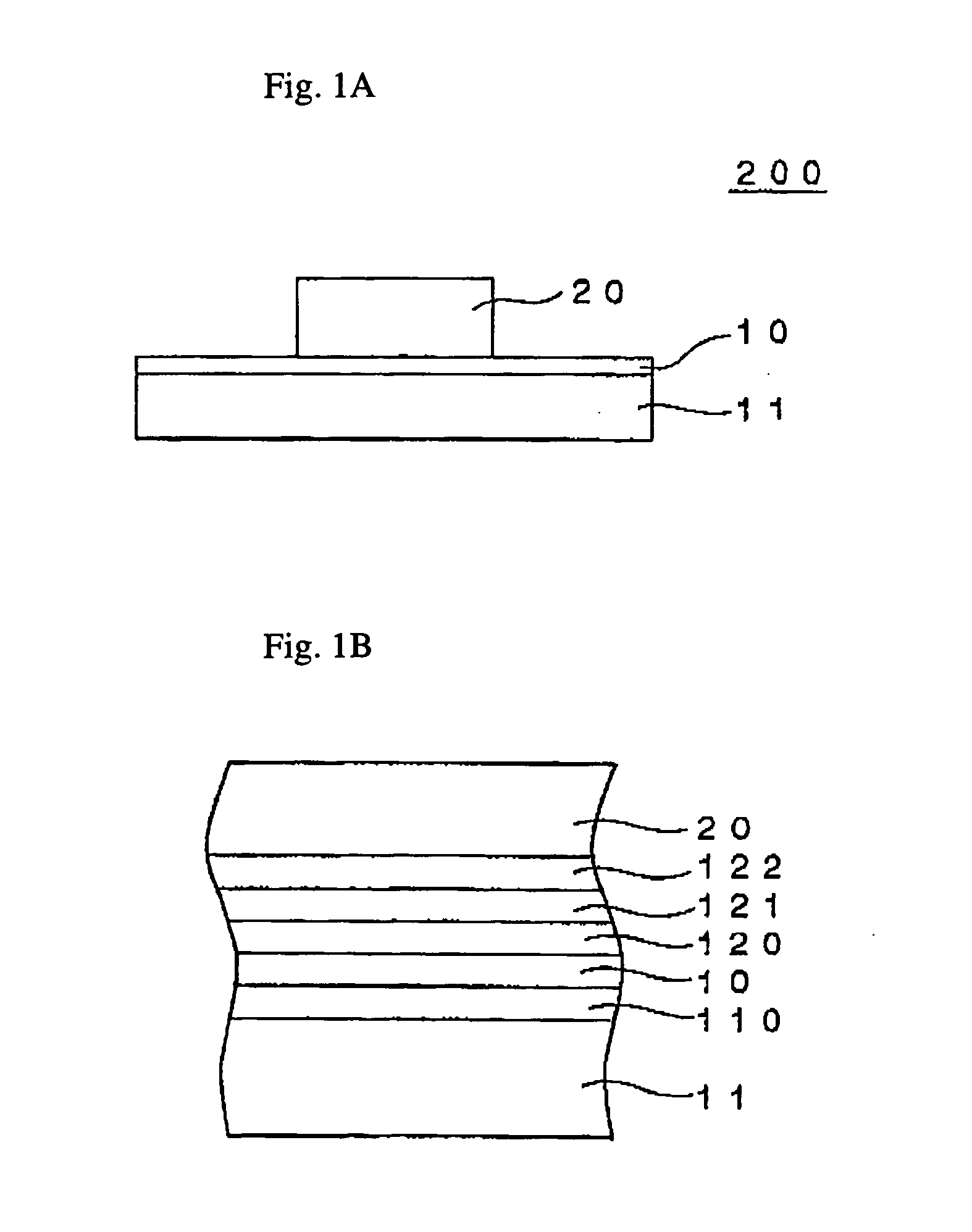
[0144] In Example 1, an example is described in which a semiconductor device with a similar structure to that of the semiconductor device shown in FIG. 1A was produced through a process of forming an electrically insulating amorphous carbon film on a conductive substrate by a plasma CVD method, and in which the semiconductor device was evaluated.

[0145] A metal plate containing 35 at. % of Cu and 65 at. % of Mo was processed to form a plate with a length of about 9 mm, a width of about 13 mm, and a thickness of 3 mm, thereby obtaining a heat dissipating plate (conductive substrate) for a semiconductor element heat dissipating member. Next, the heat dissipating plate was cleaned, and then a Cr film having a thickness of 0.2 μm was formed on one side of the heat dissipating plate by a sputtering method.

[0146] Then, the heat dissipating plate having the Cr film formed on one side thereof was laid on a sample stage in a vacuum chamber of a plasma CVD apparatus, and the vacuum chamber w...

example 2

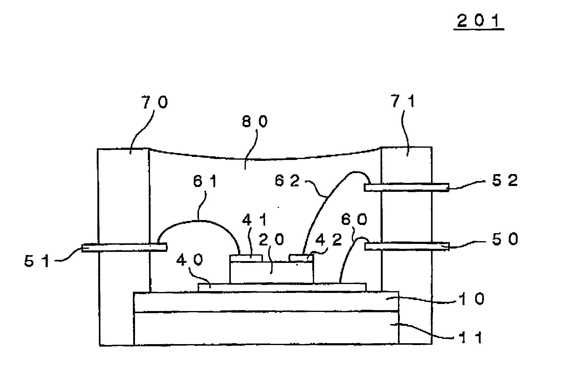
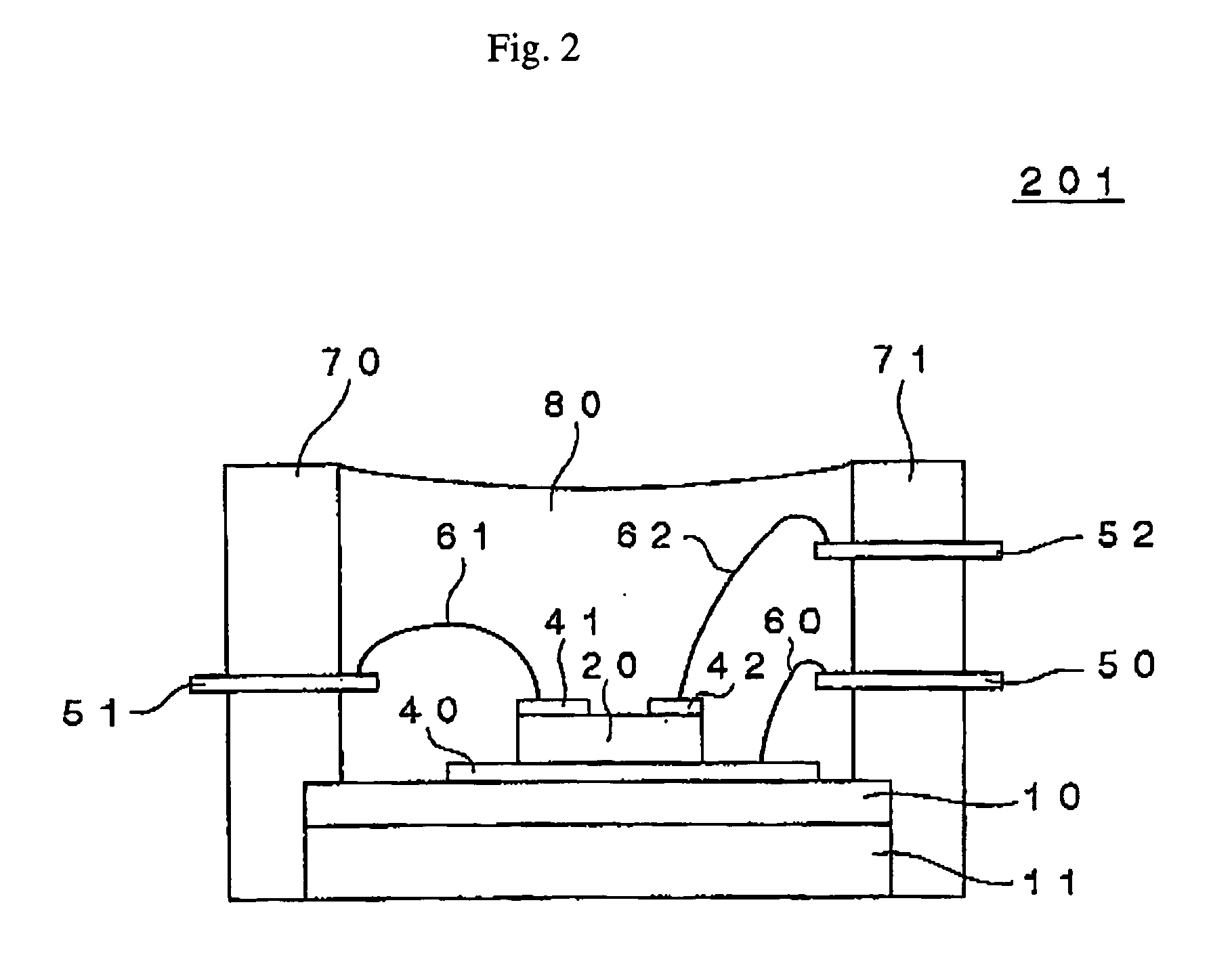
[0157] A metal plate containing 35 at. % of Cu and 65 at. % of Mo was processed to form a plate with a length of about 8 cm, a width of about 24 cm and, a thickness of 3 mm, thereby obtaining a heat dissipating plate (conductive substrate) for a semiconductor element heat dissipating member. Next, the heat dissipating plate was cleaned, and then a Cr film, an electrically insulating amorphous carbon film, an aluminum film and a Ni film were successively laminated on one side of the heat dissipating plate in the same way as in Example 1. Thereafter, six IGBT elements (with a length of about 9 mm and a width of about 12 mm) and six diodes (with a length of about 6 mm and a width of about 11 mm) were soldered thereon.

[0158] A plastic (resin block) was molded such that the plastic was disposed along the circumference of the heat dissipating plate, bus bars were provided, and electrodes disposed in contact with the IGBT elements and the diodes were connected to the bus bars by wire bond...

example 3

>Production of Semiconductor Device>

[0161] A semiconductor device of Example 3 (hereinafter, referred to as a “semiconductor device D”) was produced in the same manner as in Example 1, except that the electrically insulating amorphous carbon film was formed by using an RF plasma CVD apparatus.

[0162] The formation of the electrically insulating amorphous carbon film by using the RF plasma CVD apparatus was conducted as follows. First, the heat dissipating plate with the Cr film formed thereon was placed in the vacuum chamber of the RF plasma CVD apparatus, and the vacuum chamber was deaerated to 3×10⁻³ Pa or lower. Next, methane as a raw material gas was introduced so as to make the pressure of the vacuum chamber 13.3 Pa. Then, RF voltage of 13.56 MHz was applied to the sample stage to form the electrically insulating amorphous carbon film containing hydrogen with a thickness of 1 μm. The content of hydrogen in the electrically insulating amorphous carbon film was measured by an ERD...


PUM

PropertyMeasurementUnit
elastic modulusaaaaaaaaaa
thicknessaaaaaaaaaa
pressureaaaaaaaaaa

Abstract

A semiconductor element heat dissipating member is provided which has excellent heat dissipation characteristics and adhesion characteristics and enables production of a semiconductor device at a low cost. A semiconductor device using the same, and a method of producing the same are also provided. The semiconductor element heat dissipating member has a conductive substrate and an electrically insulating amorphous carbon film containing hydrogen, and the electrically insulating amorphous carbon film is formed at least on a region of the conductive substrate on which region a semiconductor element is to be mounted.

Description

TECHNICAL FIELD [0001] The present invention relates to a semiconductor element heat dissipating member for dissipating heat generated in semiconductor elements, a semiconductor device using the same and a production method thereof. BACKGROUND ART [0002] There is a problem of the increase in heat generation caused by development of a high-power downsized semiconductor element with an electric power control. A conventional semiconductor device forms a module in which a semiconductor element is disposed on a substrate made of an electrical insulator so as to electrically isolate the semiconductor element, and in which the electrically insulating substrate is disposed on a heat sink (a heat dissipating plate) and a cooling plate. [0003] AlN (described, for example in Japanese Patent Application Laid-Open (JP-A) No.7-99268) or Al2O3 is widely used as a heat sink material which should provide electrical insulation and thermal conductivity. [0004] An example of the structure of the semico...

Claims


Application Information

Patent Timeline
Patent Type & Authority Applications(United States)
IPC IPC(8): H01L21/44H01L23/373
CPCH01L23/3732H01L2224/49109H01L2924/13091H01L2924/1305H01L2224/48091H01L2224/48247H01L2924/13055H01L2924/19107H01L2924/3025H01L2924/00014H01L2924/00
Inventor NAKANISHI, KAZUYUKIOSHIMA, TADASHIHASEGAWA, HIDEOMORI, HIROYUKITACHIKAWA, HIDEOMIYACHI, YUKIOYAMADA, YASUSHIUEDA, HIROYUKIISHIKO, MASAYASU
Owner TOYOTA CENT RES & DEV LAB INC
Why Eureka
Try Eureka