

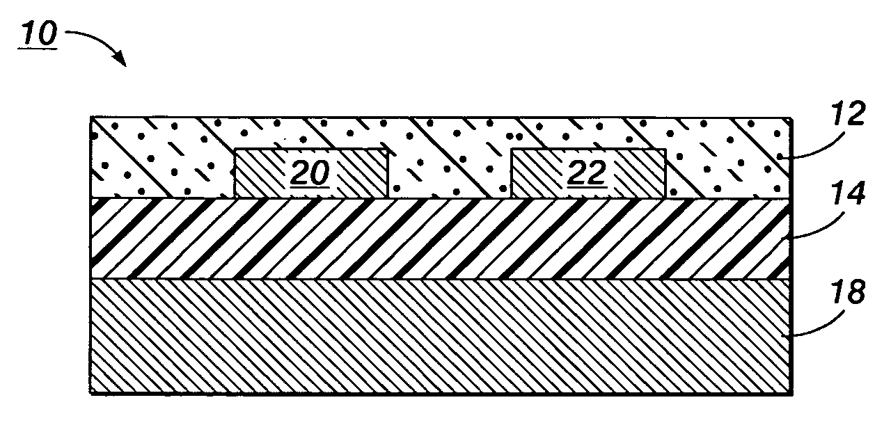
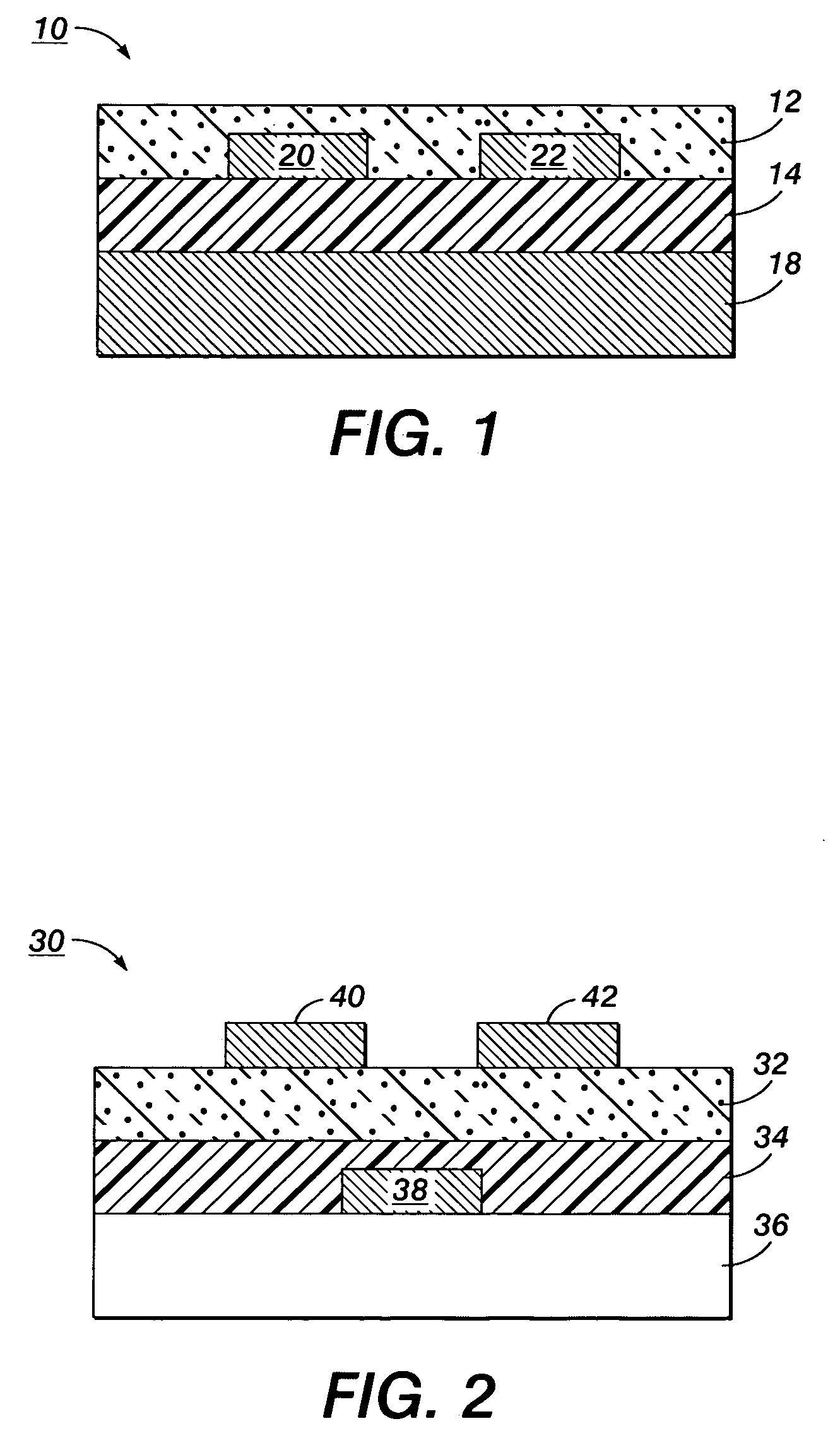
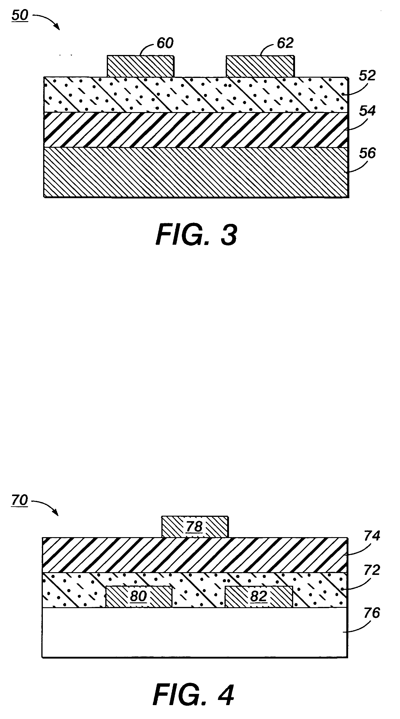
Nanoparticle deposition process
a technology of nanoparticles and deposition processes, applied in nanostructure manufacturing, transportation and packaging, layered products, etc., can solve the problems of high cost of vacuum deposition and photolithography, and is not suitable for manufacturing low-cost large-area electronics
- Summary
- Abstract
- Description
- Claims
- Application Information
AI Technical Summary
Benefits of technology
Problems solved by technology
Method used
Image

Examples
example 1
Preparation of Gold Nanoparticles with an Alkanethiol Stabilizer
[0076] To a tetraoctylammonium bromide (2.19 g, 4 mmol) solution in toluene (80 mL) in a 500 mL flask was added hydrogen tetrachloroaurate (III) trihydrate (0.394 g, 1 mmol) solution in water (100 mL) with rapid stirring (under argon). After two minutes, 1-octanethiol (0.439 g, 3 mmol) in toluene (30 mL) was added to the flask and stirred vigorously for 10 min at room temperature until the solution became colorless. Then the solution was cooled to 0° C. by an ice-water bath. A freshly prepared sodium borohydride (0.378 g, 10 mmol) solution in water (100 mL) was added to the vigorously stirred solution over 30 seconds. The reaction mixture was allowed to warm to room temperature and the rapid stirring was continued for 3 h. The organic phase was separated and concentrated to 5 mL by evaporation of the solvent (the bath temperature is <40° C.). The concentrated solution was added drop-wise to 200 mL rapidly stirring meth...
example 2
Preparation of Silver Nanoparticles with an Alkanethiol Stabilizer
[0077] Silver nanoparticles stabilized with n-octanethiol were prepared according to the procedure as described in Example 1 using silver nitrate (0.17 g, 1 mmol). A dark brown solid (0.18 g) was obtained after work-up.
example 3
Preparation of Gold Nanoparticles with Organophosphine Stabilizer
[0078] To a tetraoctylammonium bromide (1.60 g, 2.93 mmol) solution in toluene (50 mL) in a 500 mL flask was added hydrogen tetrachloroaurate (III) trihydrate (1.00 g, 2.54 mmol) solution in water (65 mL) with rapid stirring (under argon). After two minutes, triphenylphosphine (2.32 g, 8.85 mmol) was added to the flask and stirred vigorously for 10 min at room temperature. Then the solution was cooled to 0 degree C. by an ice-water bath. A freshly prepared sodium borohydride (1.41 g, 37.3 mmol) solution in water (10 mL) was added to the vigorously stirred solution over 30 seconds. The reaction mixture was allowed to warm to room temperature and the rapid stirring was continued for 3 h. The organic phase was washed with water 3 times, separated, dried over anhydrous magnesium sulfate, and filtered. The solvent was removed by evaporation (the bath temperature is <40° C.) to give a black solid. The solid was washed with ...
PUM
| Property | Measurement | Unit |
|---|---|---|
| size | aaaaa | aaaaa |
| size | aaaaa | aaaaa |
| size | aaaaa | aaaaa |
Abstract
Description
Claims
Application Information