Method of preparing cadmium sulfide nanocrystals emitting light at multiple wavelengths, and cadmium sulfide nanocrystals prepared by the method

a technology of cadmium sulfide nanocrystals and nanocrystals, which is applied in the direction of crystal growth process, discharge tube/lamp details, climate sustainability, etc., can solve the problem that the vapor deposition process is inappropriate for the fabrication of commercially viable devices

Active Publication Date: 2006-03-23
SAMSUNG ELECTRONICS CO LTD
View PDF5 Cites 46 Cited by
  • Summary
  • Abstract
  • Description
  • Claims
  • Application Information

AI Technical Summary

Benefits of technology

[0013] In accordance with one aspect of the present invention, the above objects can be accomplished by a method for preparing cadmium sulfide nanocrystals comprising the steps of: (a) mixing a cadmium precursor and a dispersant in a solvent that weakly coordinates to the cadmium precursor, and heating the mixture to obtain a cadmium precurso

Problems solved by technology

However, since quantum dots prepared by vapor deposition using the phenomenon of lattice mismatch have serious drawbacks in the control of their size, uniformity, density, etc

Method used


Image

  • Method of preparing cadmium sulfide nanocrystals emitting light at multiple wavelengths, and cadmium sulfide nanocrystals prepared by the method
  • Method of preparing cadmium sulfide nanocrystals emitting light at multiple wavelengths, and cadmium sulfide nanocrystals prepared by the method
  • Method of preparing cadmium sulfide nanocrystals emitting light at multiple wavelengths, and cadmium sulfide nanocrystals prepared by the method

Examples


example 1

Preparation of Cadmium Sulfide Nanocrystals, and Fabrication of White Light-Emitting Diode

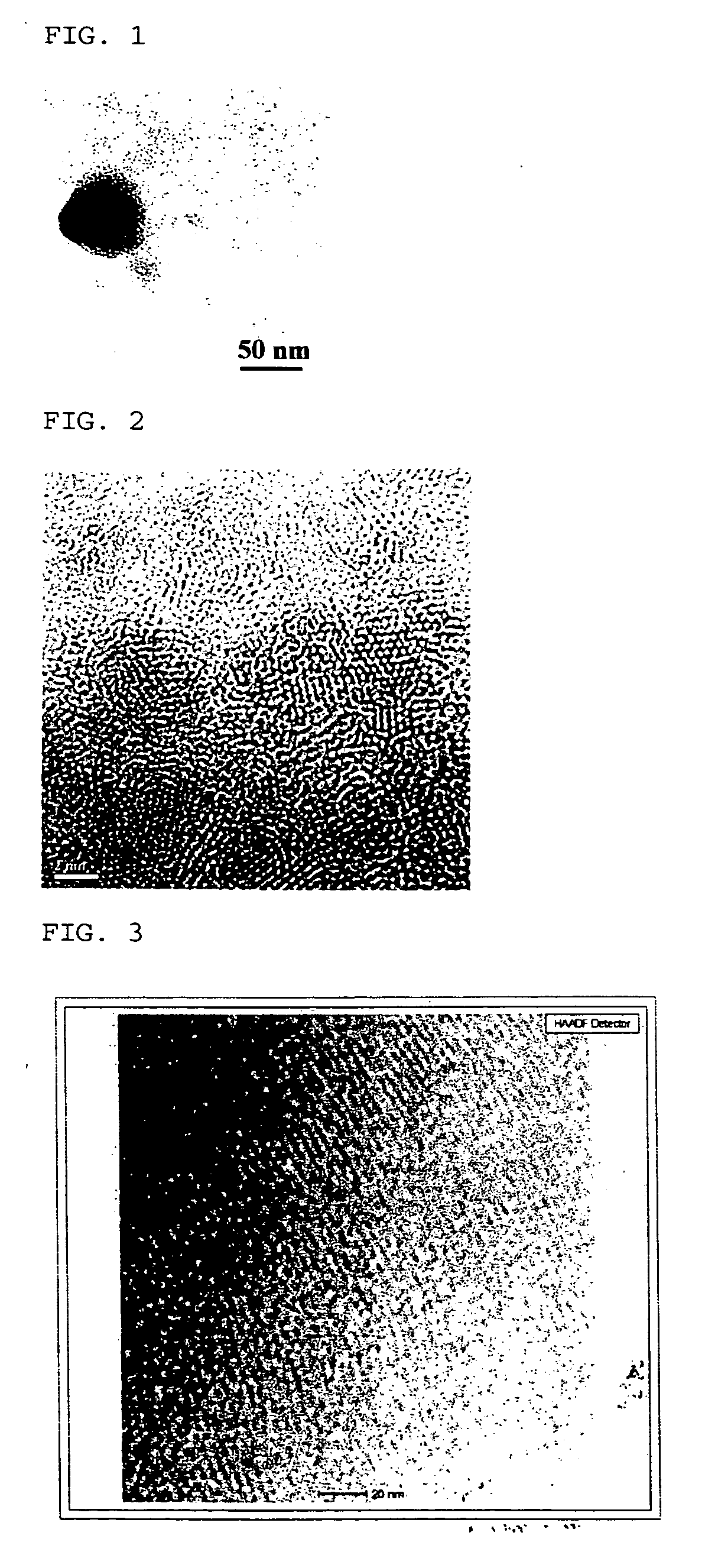
[0063] 16 g of octadecene, 2 g of oleic acid, and 0.4 mmol of cadmium oxide (CdO) as a cadmium precursor were simultaneously charged into a 100 ml flask equipped with a reflux condenser. The reaction mixture was heated to 300° C. while stirring and maintaining the mixture under nitrogen atmosphere at a constant pressure to avoid the generation of a temperature gradient in the mixture. The heated reaction mixture was steadily stirred at the same temperature until the original color (red) of the cadmium oxide became transparent.

[0064] Separately, a sulfur powder as a sulfur precursor was added to octadecene, and then the resulting reaction mixture was heated to 250° C. using a heating mantle while stirring and maintaining the mixture under nitrogen atmosphere at a constant pressure to avoid the generation of a temperature gradient in the mixture. The heated reaction mixture was steadily stirred...


PUM

PropertyMeasurementUnit
Temperatureaaaaaaaaaa

Abstract

A method for preparing cadmium sulfide nanocrystals emitting light at multiple wavelengths. The method comprises the steps of (a) mixing a cadmium precursor and a dispersant in a solvent that weakly coordinates to the cadmium precursor, and heating the mixture to obtain a cadmium precursor solution, (b) dissolving a sulfur precursor in a solvent that weakly coordinates to the sulfur precursor to obtain a sulfur precursor solution, and (c) feeding the sulfur precursor solution to the heated cadmium precursor solution maintained at a high temperature to prepare cadmium sulfide crystals, and growing the cadmium sulfide crystals. Further, cadmium sulfide nanocrystals prepared by the method. The cadmium sulfide nanocrystals have uniform size and shape and can emit light close to white light simultaneously at different wavelengths upon excitation. Due to these characteristics, the cadmium sulfide nanocrystals can be applied to white light-emitting diode devices.

Description

[0001] This non-provisional application claims priority under 35 U.S.C. § 119(a) on Korean Patent Application No. 2004-38392 filed on May 28, 2004, which is herein expressly incorporated by reference in its entirety. BACKGROUND OF THE INVENTION [0002] 1Field of the Invention [0003] The present invention relates to a method for preparing cadmium sulfide nanocrystals emitting light at multiple wavelengths, and cadmium sulfide nanocrystals prepared by the method. More particularly, the present invention relates to a method for preparing cadmium sulfide nanocrystals by mixing a cadmium precursor and a dispersant in a solvent that weakly coordinates to the cadmium precursor, heating the mixture to obtain a cadmium precursor solution, dissolving a sulfur precursor in a solvent that weakly coordinates to the sulfur precursor to obtain a sulfur precursor solution, feeding the sulfur precursor solution to the heated cadmium precursor solution maintained at a high temperature to prepare cadmi...

Claims


Application Information

Patent Timeline
IPC IPC(8): C01G11/02C09K11/56H01L33/28H05B33/14
CPCB82Y30/00Y10S362/80C01P2002/84C01P2004/03C01P2004/04C01P2004/64C09K11/565C30B7/00C30B29/50C30B29/60H01L33/28H05B33/14Y02B20/181Y10S977/773Y10S977/775C01G11/02Y02B20/00
Inventor JANG, EUN JOOJUN, SHIN AEAHN, TAE KYUNGLEE, SUNG HUNCHOI, SEONG JAE
Owner SAMSUNG ELECTRONICS CO LTD
Why Eureka
Try Eureka