Method of manufacturing a semiconductor device

a manufacturing method and semiconductor technology, applied in semiconductor devices, capacitors, electrical devices, etc., can solve the problems of node electrode collapse, node electrode collapse, and inability to improve the structure of storage node electrodes, etc., to reduce the step between the cell area and the peripheral area

Inactive Publication Date: 2006-03-23
SAMSUNG ELECTRONICS CO LTD
View PDF12 Cites 32 Cited by
  • Summary
  • Abstract
  • Description
  • Claims
  • Application Information

AI Technical Summary

Benefits of technology

[0018] Embodiments of the present invention provide a method of manufacturing a semiconductor device that solves the problems cited above by reducing a step between the cell area and the peripheral area.
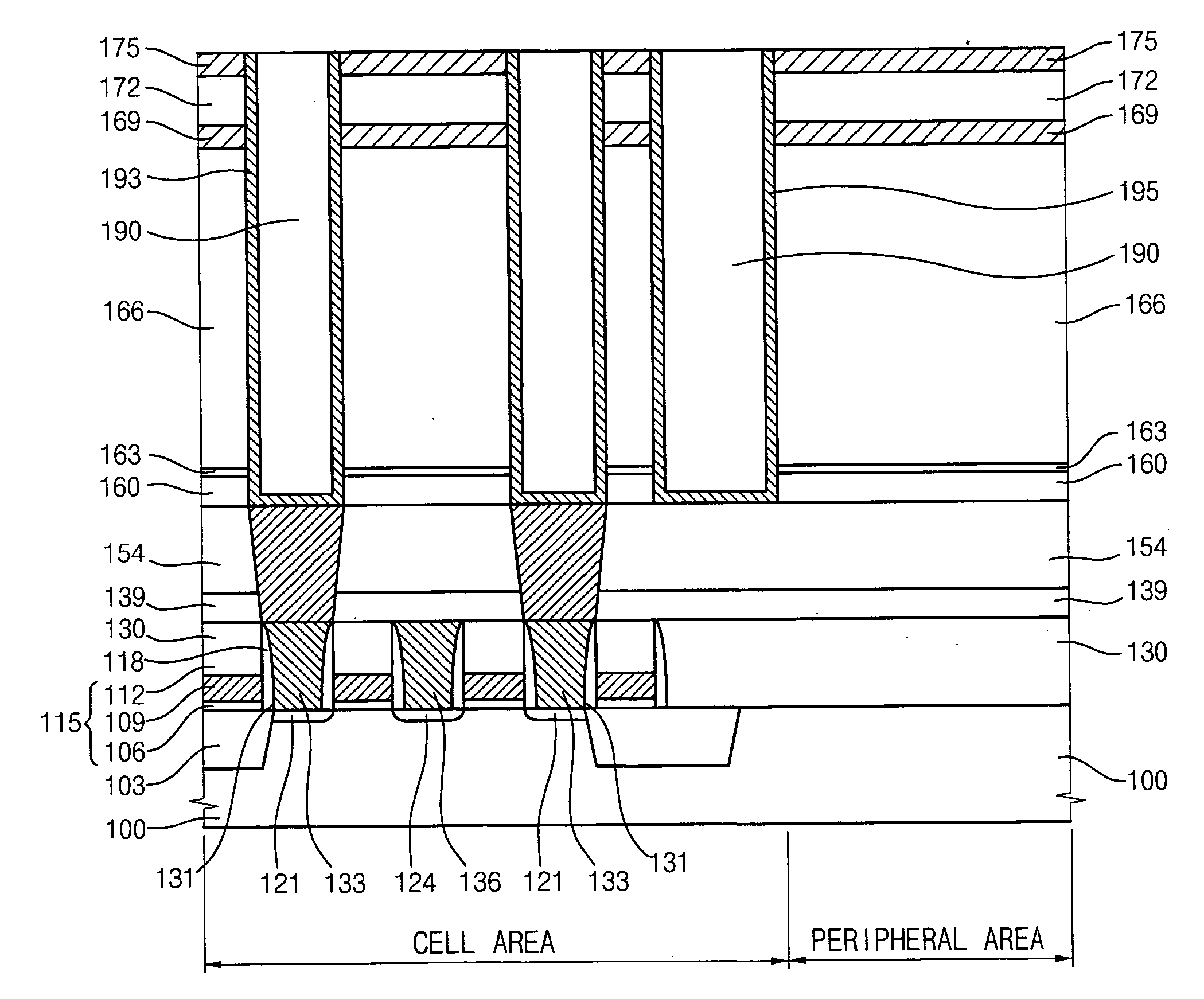
[0019] In a method of manufacturing a semiconductor device in accordance with one aspect of the present invention, a first opening and a second opening are formed through a plurality of thin layers including a support layer on a substrate. The first opening through which a top surface of a contact pad is exposed is formed in a cell area of the substrate, and the second opening is formed in a boundary region of the cell area and a peripheral area of the substrate. A storage electrode is formed on a sidewall and a bottom of the first opening, and a guide ring is formed on a sidewall and a bottom of the second opening by removing a conductive layer formed along the sidewalls and bottoms of the first and second openings. A support pattern is formed by etching the thin layers so that the support layer in the cell area is partially etched and the support layer in the peripheral area remains un-etched to thereby be exposed, so that the support pattern supports and surrounds a plurality of storage electrodes adjacent to each other in the cell area and prevents a layer underlying the support layer from being etched in the peripheral area. A dielectric layer and a plate electrode are sequentially formed on the storage electrode to thereby complete a semiconductor device that is capable of reducing a step between the cell area and the peripheral area.

Problems solved by technology

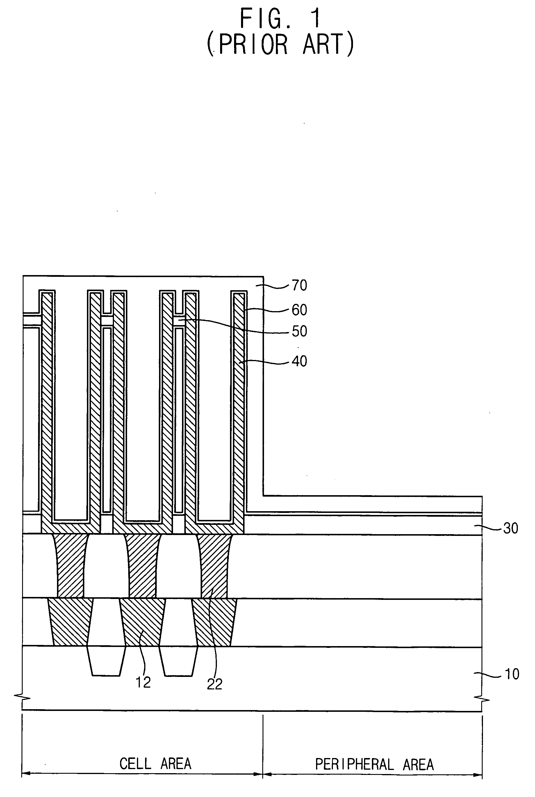
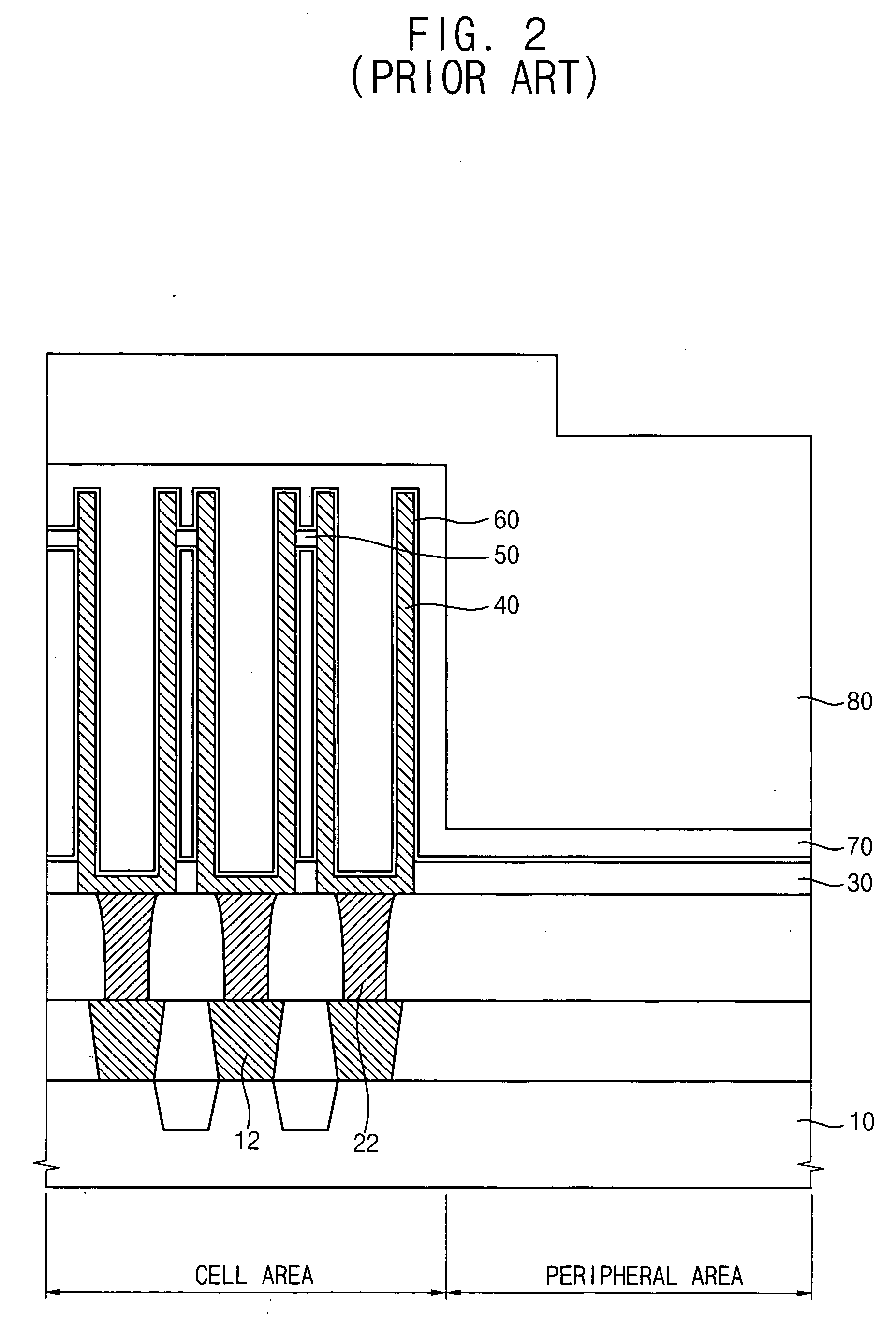
Attempting to increase the capacitance by improving the structure of the storage node electrode, however, is restricted due to a limit of a design rule, increases of error ratios caused by complicated processes, etc.
As a result, most attempts are regarded skeptically with respect to the possibility of producing a capacitor having the above-mentioned structures.
However, the storage node electrode collapses due to its increased height, creating an electrical bridge between adjacent storage node electrodes.
Also, the planarization process is expensive.
As a result, the photolithography process, the dry etching process, and the planarization process of the conventional methods for forming the capacitor are complicated and costly.

Method used


Image

  • Method of manufacturing a semiconductor device
  • Method of manufacturing a semiconductor device
  • Method of manufacturing a semiconductor device

Examples


first modified embodiment

[0099]FIG. 29 is a plan view illustrating the second opening shown in FIG. 9.

[0100] Although the above exemplary embodiment describes the second opening 185 formed around the cell region and surrounding the cell region with a uniform width shown in FIG. 9, the second opening can be modified so that its width is varied in accordance with the metal contact plug 217. In the present embodiment, the second opening is modified so that a corner portion thereof has a sufficient width to hold the metal contact plug 217 and a remaining portion, except the corner portion, has a relatively small width, as shown in FIG. 29.

second modified embodiment

[0101]FIG. 30 is a plan view illustrating the second opening shown in FIG. 9, and FIG. 31 is a plan view illustrating another modified embodiment of the first embodiment of the second opening shown in FIG. 29.

[0102] Referring to FIG. 30, the second opening 185 shown in FIG. 9 is otherwise modified so that a plurality of protruding portions 186 is formed in the second opening 185. The protruding portion 186 is vertically protruded from a bottom surface of the second opening 185. In a similar way, the first modified embodiment of the second opening 185a is re-modified so that a plurality of protruding portions 186a is formed in the corner portion of the first modified embodiment of the second opening 185a. The protruding portion 186a is vertically protruded from a bottom surface of the first modified embodiment of the second opening 185a. The protruding portion 186 and 186a facilitates a filling of the second opening 185 and the first modified embodiment of the second opening 185a wit...


PUM


Abstract

In an embodiment, a simplified method of manufacturing a semiconductor device reduces a step between cell and peripheral areas. First and second openings are formed through a plurality of thin layers including a support layer on a substrate. A storage electrode and a guide ring are formed on sidewalls and bottoms of the first and second openings, respectively. A support pattern is formed so that the support layer in the cell area is partially etched and the support layer in the peripheral area remains un-etched, thus the support pattern supports and surrounds the storage electrodes adjacent to each other in the cell area and prevents an etching of a layer underlying the support layer in the peripheral area. A dielectric layer and a plate electrode are formed on the storage electrode to complete a semiconductor device with the reduced step.

Description

CROSS REFERENCE TO RELATED APPLICATION [0001] This application claims priority under 35 USC § 119 to Korean Patent Application No. 2004-50191, filed on Jun. 30, 2004, the contents of which are incorporated herein by reference in its entirety. BACKGROUND OF THE INVENTION [0002] 1. Field of the Invention [0003] The present invention relates to a method of manufacturing a semiconductor device. More particularly, the present invention relates to a method of manufacturing a semiconductor device that includes a cylindrical capacitor. [0004] 2. Description of the Related Art [0005] Higher cell capacitance is often used to improve characteristics of a memory cell in a dynamic random access memory (DRAM) device. The increased cell capacitance improves read-out capacity of the memory cell and reduces soft errors. Meanwhile, as semiconductor memory devices have become more highly integrated, the unit memory cell of the semiconductor memory device has continuously decreased in area. As a result...

Claims


Application Information

Patent Timeline
Patent Type & Authority Applications(United States)
IPC IPC(8): H01L21/8242H01L27/02H01L27/108
CPCH01L27/0207H01L27/10814H01L28/91H01L27/10882H01L27/10894H01L27/10852H10B12/315H10B12/48H10B12/09H10B12/033H10B99/00
Inventor PARKJEONG, SANG-SUP
Owner SAMSUNG ELECTRONICS CO LTD
Why Eureka
Try Eureka