Process for producing p doped silicon single crystal and p doped n type silicon single crystal wafer

Active Publication Date: 2006-03-30
SHIN-ETSU HANDOTAI CO LTD
View PDF0 Cites 13 Cited by
  • Summary
  • Abstract
  • Description
  • Claims
  • Application Information

AI Technical Summary

Benefits of technology

[0028] If the wafer is that the whole plane of the wafer is N region and/or I region as described above, because I region is also defect-free in the P-doped N-type silicon single crystal wafer of the present invention, the wafer can be easily and inexpensively produced. And it can have an excellent electrical characteristics to be high breakdown voltage.
[0029] As explained above, according to the present invention, because I region becomes a defect-free region by doping the prescribed amount of

Problems solved by technology

It is difficult to control the rate because the single crystal of N region can be grown in a range

Method used


Image

  • Process for producing p doped silicon single crystal and p doped n type silicon single crystal wafer
  • Process for producing p doped silicon single crystal and p doped n type silicon single crystal wafer
  • Process for producing p doped silicon single crystal and p doped n type silicon single crystal wafer

Examples


example 1

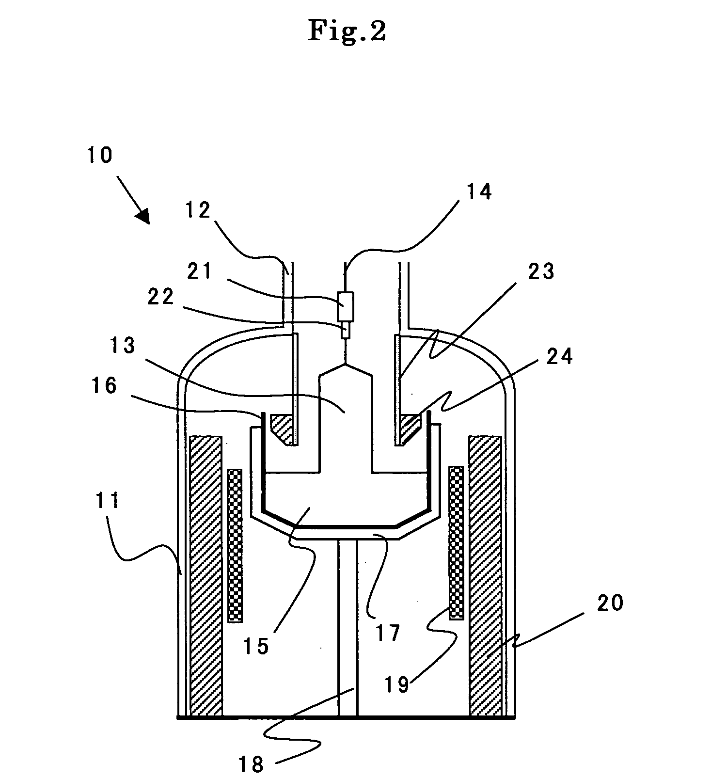
[0047] A silicon single crystal was produced by using a single crystal production apparatus as shown in FIG. 2. 150 kg of raw material polycrystal silicon and 4 mg of refined Al metal grains were charged in the quartz crucible with a diameter of 24 inches (600 mm), and a silicon single crystal with a diameter of 210 mm and orientation was pulled. When pulling the silicon single crystal, a growth rate was controlled so as to be gradually decreased from a head of the crystal through a tail thereof in a range from 0.60 mm / min to 0.20 mm / min. Moreover, the silicon single crystal was produced so that a P concentration might be 3×10¹⁴ to 5.5×10¹⁴ atoms / cc and oxygen concentration might be 24-27 ppma (ASTM'79).

[0048] A straight body of each silicon single crystal ingot grown as described above was cut into blocks by each length of 10 cm along a crystal growth axis as shown in FIG. 3(a), and thereafter each block was cut longitudinally along the crystal axis and several samples with thick...

example 2

[0056] A silicon single crystal was produced and each measurement was performed as the same with Example 1 except for charging 150 kg of raw material polycrystal silicon and 8 mg of refined Al metal grains in a quartz crucible.

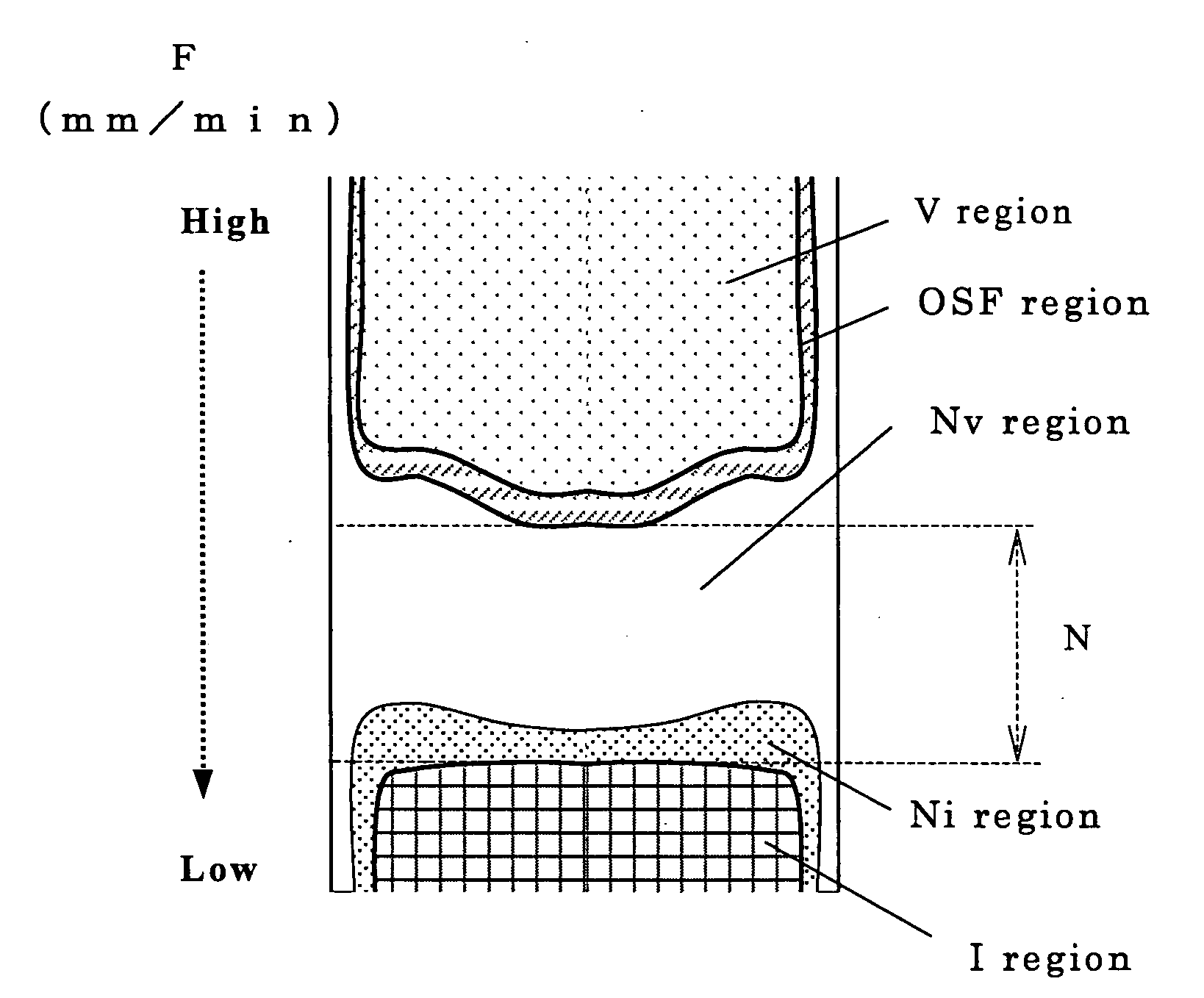
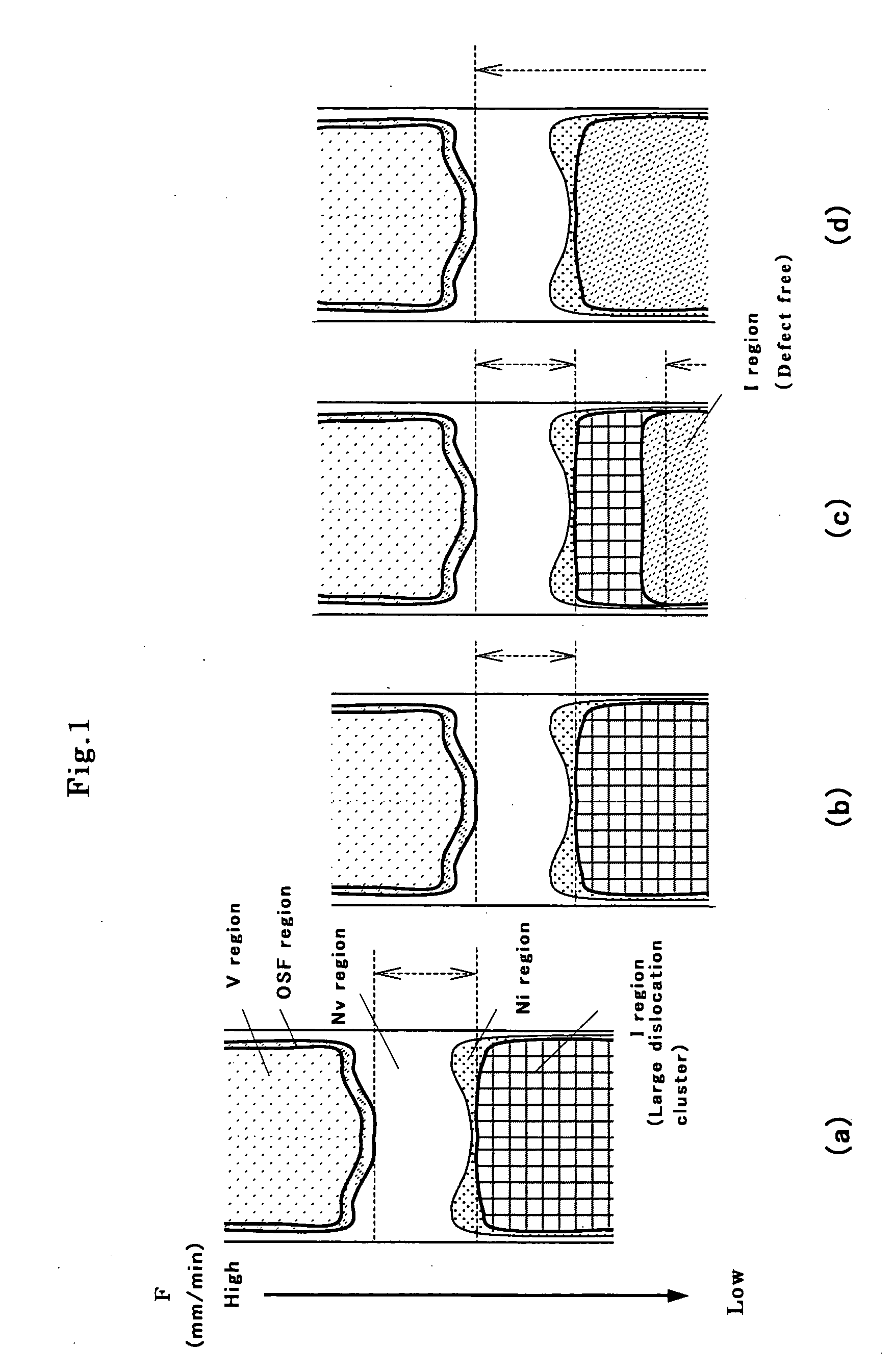
[0057] More detailed distribution of each region which was found from the above-described measurement is shown in FIG. 1 (d). F / G (mm2 / ° C.·min) and an Al concentration in each region boundary are shown as follows.

[0058] F / G (mm2 / ° C.·min) in the boundary between OSF region and N region: 0.20

[0059] F / G (mm2 / ° C.·min) in the boundary between N region and (defect-free) I region: 0.18 an Al concentration in the crystal bulk near

[0060] F / G=0.17:8.8×10¹² atoms / cc.


PUM


Abstract

The present invention is a method of producing a P(phosphorus)-doped silicon single crystal by Czochralski method, wherein, at least, a growth of the single crystal is performed so that an Al (aluminum) concentration is 2×10¹² atoms/cc or more. Thereby, there can be provided a method of easily and inexpensively producing a P(phosphorus)-doped silicon single crystal of defect-free region having an excellent capability of electrical characteristics to be high breakdown voltage, which contains neither, for example, V region, OSF region, nor large dislocation cluster (LSEPD, LFPD) region.

Description

TECHNICAL FIELD [0001] The present invention relates to a method of producing a P-doped silicon single crystal by Czochralski method and a P-doped N-type silicon single crystal wafer. Particularly, the present invention relates to a method of producing a P-doped silicon single crystal of defect-free region having an excellent capability of electrical characteristics to be high breakdown voltage, which contains neither V region, OSF region, nor large dislocation cluster (LSEPD, LFPD) region, and to a P-doped N-type silicon single crystal wafer. BACKGROUND ART[0002] A single crystal used as a substrate of semiconductor devices, for example, a silicon single crystal, is mainly produced by Czochralski method (hereafter abbreviated to CZ method). [0003] When producing a single crystal by CZ method, for example, a single crystal production apparatus 10 as shown FIG. 2 is used to produce the single crystal. This single crystal production apparatus 10 has a member for containing and melting...

Claims


Application Information

Patent Timeline
IPC IPC(8): C30B15/00C30B21/06C30B27/02C30B28/10C30B30/04C30B15/04C30B29/06
CPCC30B15/04C30B29/06C30B15/203H01L21/20
Inventor SAKURADA, MASAHIROFUSEGAWA, IZUMI
Owner SHIN-ETSU HANDOTAI CO LTD
Why Eureka
Try Eureka