

Semiconductor device and method for fabricating the same
a technology of semiconductors and semiconductors, applied in the direction of semiconductor devices, electrical devices, transistors, etc., can solve the problems of difficult to prevent the decrease of processing precision, the effect of reducing the capacitance, etc., and deteriorating, etc., to achieve the effect of reducing parasitic capacitance, high performance, and not impairing the effect of soi structur
- Summary
- Abstract
- Description
- Claims
- Application Information
AI Technical Summary
Benefits of technology
Problems solved by technology
Method used
Image

Examples
first embodiment
A First Embodiment
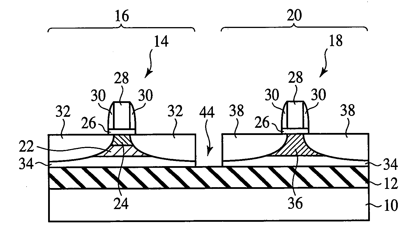
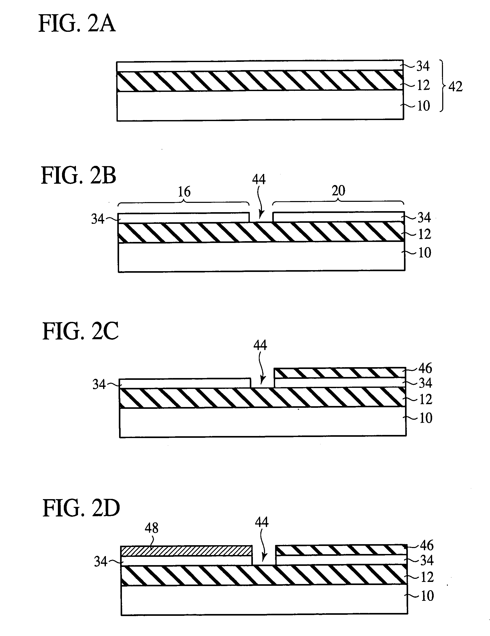
[0050] The semiconductor device and the method for fabricating the same according to a first embodiment of the present invention will be explained with reference to FIGS. 1 to 5D. FIG. 1 is a sectional view of the semiconductor device according to the present embodiment, which illustrates a structure thereof. FIGS. 2A to 5D are sectional views of the semiconductor device according to the present embodiment in the steps of the method for fabricating the same, which illustrate the method.
[0051] First, the structure of the semiconductor device according to the present embodiment will be explained with reference to FIG. 1.
[0052] An insulation layer 12 of silicon oxide film is formed on a silicon substrate 10.
[0053] On the silicon substrate 10 with the insulation film 12 formed on, an NMOS transistor region 16 where an NMOS transistor 14 is formed and a PMOS transistor region 20 where a PMOS transistor 18 is formed are provided. The NMOS transistor region 16 and the ...
second embodiment
A Second Embodiment
[0101] The semiconductor device and the method for fabricating the same according to a second embodiment of the present invention will be explained with reference to FIGS. 6 to 8D. FIG. 6 is a sectional view of the semiconductor device according to the present embodiment, which illustrates a structure thereof. FIGS. 7A to 8D are sectional views of the semiconductor device according to the present embodiment in the steps of the method for fabricating the same, which illustrate the method. The same members of the present embodiment as those of the semiconductor device and the method for fabricating the same according to the first embodiment are represented by the same reference numbers not to repeat or to simplify their explanation.
[0102] The structure of the semiconductor device according to the present embodiment is basically substantially the same as that of the semiconductor device according to the first embodiment. The semiconductor device according to the pre...
third embodiment
A Third Embodiment
[0116] The method for fabricating the semiconductor device according to a third embodiment of the present invention will be explained with reference to FIGS. 9A to 15B. FIGS. 9A-9D and 14A-14D are sectional views of the semiconductor device according to the present embodiment in the steps of the method for fabricating the same, which illustrate the method. FIGS. 10A and 10B are graphs of the Raman spectra of the silicon germanium layer before and after the application of a laser beam. FIGS. 11A and 11B are views explaining the relationship between the thickness of the silicon oxide film and the reflectance of a laser beam. FIG. 12 is a view explaining the relationship between the wavelength of a laser beam and the lattice relaxation. FIG. 13 is a graph schematically showing the relationship between the thickness of the silicon germanium layer and the lattice relaxation by the application of a laser beam. FIGS. 15A and 15B are views of the evaluation results. The sa...
PUM
 Abstract
Description
Claims
Application Information