Optical information recording medium, reproducing method thereof, and manufacturing method thereof

Inactive Publication Date: 2006-04-06
HITACHI LTD
View PDF2 Cites 47 Cited by
  • Summary
  • Abstract
  • Description
  • Claims
  • Application Information

AI Technical Summary

Benefits of technology

[0059] The present invention makes it possible to read out data recorded on an optical disk possessing a capacity of approximately 100 gigabytes per surface, while utilizing a sy

Problems solved by technology

These pits cannot be separated and reading out their data is impossible.
The reason for the improved S/N ratio is that, in conventional

Method used


Image

  • Optical information recording medium, reproducing method thereof, and manufacturing method thereof
  • Optical information recording medium, reproducing method thereof, and manufacturing method thereof
  • Optical information recording medium, reproducing method thereof, and manufacturing method thereof

Examples


first embodiment

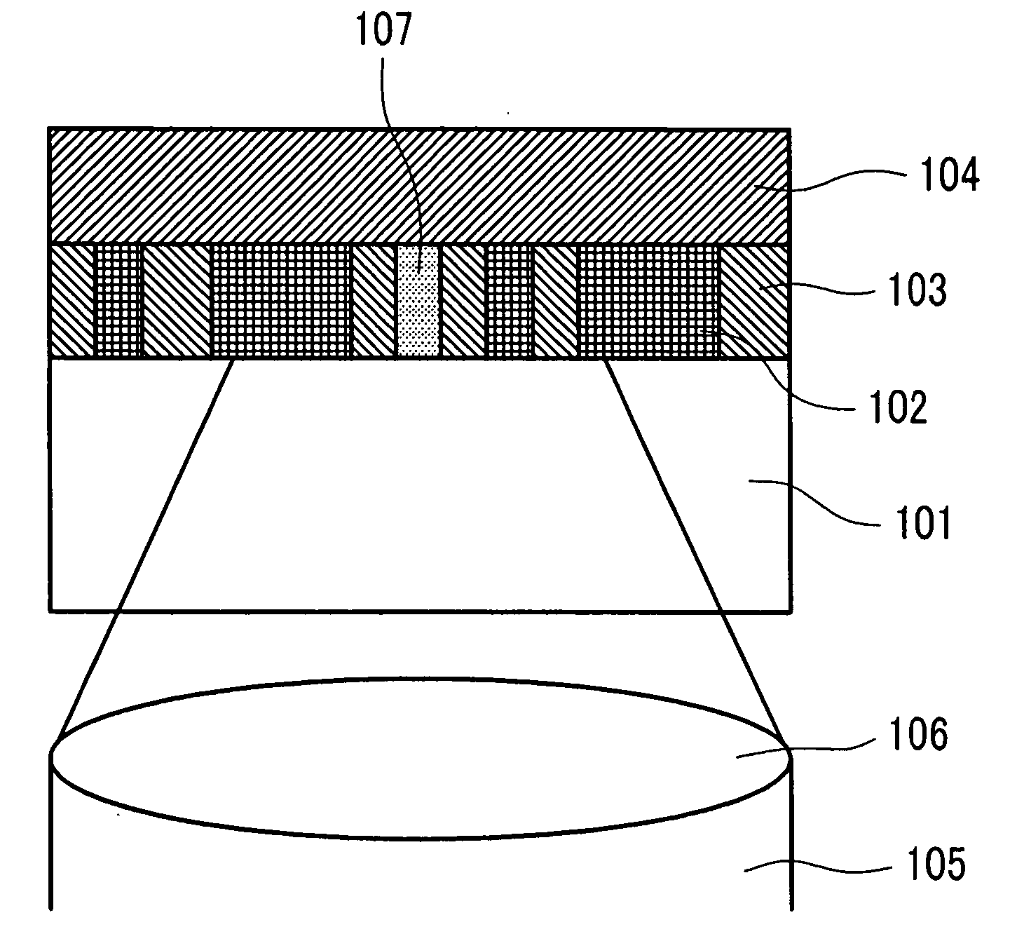
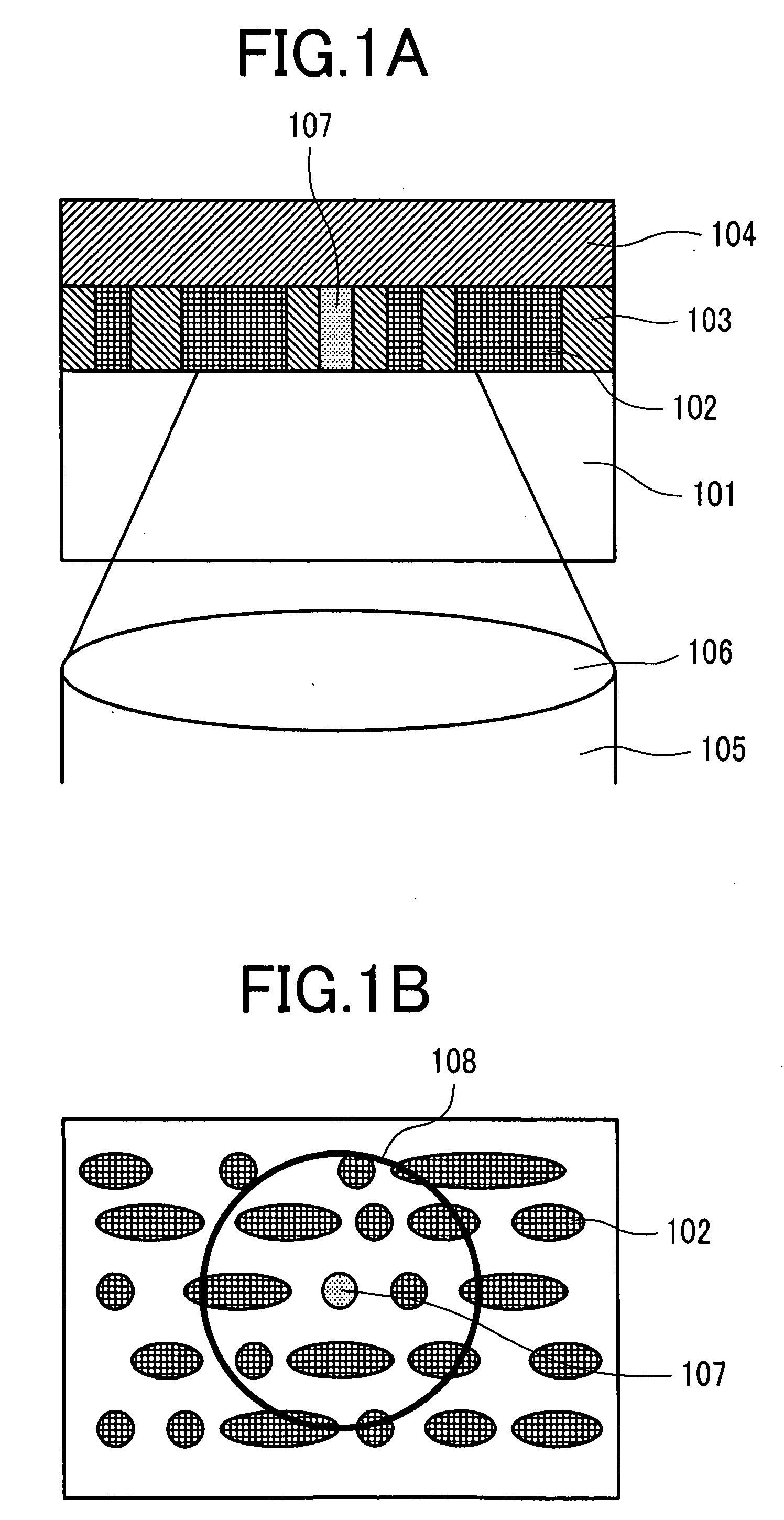
[0103] A single layer disk was fabricated to evaluate the effect of the present invention. The disk was fabricated by utilizing the method shown in FIGS. 6A-6I. An upper substrate in FIGS. 6A-6I is made from polycarbonate and has a thickness of 1.2 mm. A reflective film 605 is made from silver (Ag) and has a thickness of 20 nm. An upper protective film 604 is made from ZnS—SiO2 and has a thickness of 30 nm. A phase-change film 603 is made from Ge5Sb70Te25 and has a thickness of 20 nm. A lower protective film 602 is made from SiO2 and has a thickness of 55 nm. A lower substrate 601 is provided as a 0.1 mm thick sheet of polycarbonate and is bonded by UV curable resin. The structure of that film is shown in FIG. 3A and the signal evaluation function calculated at the maximum is shown in FIG. 3B. The films were all formed by sputtering. The films were sputtered on the upper substrate 606 in the sequence of the reflective upper protective film, the phase-change film, and the lower prote...

second embodiment

[0117] Data on the disk fabricated by the method shown in FIG. 7 was read out and the error rate measured.

[0118] The method described in the first embodiment was utilized to record the data on the disk. The (1,7) modulation method was used for modulation coding, and the shortest mark length was set at 40 nm. A disk was fabricated using the method shown in FIGS. 6A-6I in connection with the first embodiment. The state shown in FIG. 6E, however, was used for the mold utilizing a CV curable resin, and that resin was plated with nickel to obtain the master disk. A stamper of nickel was made from this master disk. On the other hand, Ag having a thickness of 20 nm, ZnS—SiO2 having a thickness of 30 nm, and Ge2SbsTe5 serving as a phase-change material and having a thickness of 20 nm was sputtered onto a 1.2 mm thick polycarbonate substrate. A nickel stamper heated to 200° C. was brought into contact with the sample material for one second to form a crystallized mark pattern on the sample ...

third embodiment

[0121] Data from the disk fabricated by the method shown in FIGS. 9A-9H was read out here.

[0122] The methods described in conjunction with the first embodiment and the second embodiment were utilized to record data onto the disk. A sodium hydroxide solution at pH12 was coated on the surface of the sample material in FIG. 9A by utilizing a spin coater. The solution of sodium hydroxide at this time covers a radial section from 20 to 60 mm on the surface of the disk. This section has a surface area of approximately 0.01 m2. This sample material is moistened in 16 milligrams of stearic acid. This section was measured beforehand with 24 milligrams of stearic acid covering a surface area of 0.01 m2 with no gaps. The stearic acid has a diameter of approximately 1 nm, and, further, it has a molecular weight of 284, so that the weight of stearic acid described above is largely a suitable value. At this point in time, two-thirds of the surface from a radius of 20 to 60 mm on the disk, is cov...


PUM


Abstract

Super-resolution technology was proposed for generating marks smaller than the optical resolution in order to record data at high density on the optical disk. However, the achievable high density of the super-resolution technology was limited due to fluctuation of the region exhibiting the super-resolution effect due to the grain size or the molecular size comprising the super-resolution film. However fluctuation in the region exhibiting the super-resolution effect is reduced by utilizing recording marks possessing their own super-resolution effect and also by separating the recording marks from each other.

Description

CLAIM OF PRIORITY [0001] The present invention claims priority from Japanese application JP 2004-290891, filed on Oct. 4, 2004, the content of which is hereby incorporated by reference into this application. FIELD OF THE INVENTION [0002] The present invention relates to technology for high density optical disks. BACKGROUND OF THE INVENTION [0003] Currently, research and development efforts are making advances in technology for achieving high density optical recording that is capable of storing large quantities of information per unit of surface area. In products currently utilizing optical disk technology, a laser light is irradiated through a lens onto a disk, and the data recorded on the disk is then reproduced and / or recorded. Up until now, in order to record data at high densities, technology has been developed for reducing the size of the focused laser beam spot. The spot size was proportional to λ / NA, where the wavelength of the light source is λ and NA is the numerical apertu...

Claims


Application Information

Patent Timeline
IPC IPC(8): G11B7/24G11B7/24035G11B7/24038G11B7/24065G11B7/24085G11B7/243G11B7/2433
CPCG11B7/24G11B7/24038G11B7/26
Inventor SHINTANI, TOSHIMICHIMIYAMOTO, HARUKAZUANZAI, YUMIKOKUDO, HIROMI
Owner HITACHI LTD
Why Eureka
Try Eureka