Lenslet/detector array assembly for high data rate optical communications

a technology of optical communication and detector array, applied in the field of optical communication, can solve the problems of poor optical quality receiver, limited effectiveness of such devices, and original laser beam expansion and distortion, and achieve the effects of high data rate, low circuit capacitance, and high bandwidth

Inactive Publication Date: 2006-04-13
THE BOEING CO
View PDF19 Cites 86 Cited by
  • Summary
  • Abstract
  • Description
  • Claims
  • Application Information

AI Technical Summary

Benefits of technology

[0007] Another embodiment of the invention includes a method of converting a high-data rate optical signal extending over a two-dimensional spot into a high-data rate electrical signal. The method may include: focusing the optical signal onto a photodetector array; converting the optical signal into a plurality of electrical signals; disposing a transimpedance amplifier assembly to amplify each of the plurality of electrical signals; and summing each of the amplified electrical signals, to produce a summed electrical signal representative of the optical signal over the two-dimensional spot.
[0008] A further embodiment of the invention includes a method of converting a high-data rate optical signal extending over a two-dimensional spot into a high-data rate electrical signal. The method may include: focusing the optical signal onto a photodetector array; converting the optical signal into a plurality of electrical signals; disposing a summing amplifier assembly to sum each of the plurality of electrical signals; and disposing a transimpedance amplifier assembly to amplify the sum of each of the plurality of electrical signals, to produce a summed electrical signal representative of the optical signal over the two-dimensional spot.
[0009] Some embodiments provide an optical receiver assembly that may be used to collect the largest practical amount of laser energy transmitted across a free-space region from a transmitter. Near the focus of the receiver, the assembly may include an optical element or array of optical elements placed near the detector array that have a size sufficient to capture and further concentrate the optical energy contained in the blurred optical spot. The captured optical energy is focused to a photodetector array that has a series of small photodetection elements of relatively low circuit capacitance. In some examples, InGaAs photodiodes are used. In some examples, the electrical signals from these photodetectors are collected and either summed and then amplified or amplified individually and then summed by a series of high bandwidth transimpedance amplifiers. Different types of transimpedance amplifiers architectures may be used. For example, CMOS fabricated singled-ended or differential transimpedance amplifiers may be used to achieve high bandwidths and thus high data rates, for example 1 Gbit / s or higher. In some examples, the summing circuitry and transimpedance amplification can support data rates high enough to support high-definition modulated information to produce an optical communication that can receive free-space high definition video signals modulated on a laser signal.
[0010] Optical assemblies may be used in remote communication environments where signal intensities are generally quite low. Further, the optical assemblies may be used in portable, field-deployed applications along with optical receivers and wavefront correction elements.

Problems solved by technology

Yet, the size of existing communications equipment has limited the effectiveness of such devices.
Over great travel distances, however, the original laser beam will expand and distort in response to anomalies in the air medium through which the beam travels.
Additionally, atmospheric turbulence and poor optical quality receivers prevent the laser beam from being focused to a point at the remote location.
Larger optical receivers, however, increase weight and reduce portability—two things undesirable for remote deployable receivers.
Larger detectors also slow receiver responsiveness, because the intrinsic capacitance of larger detectors is larger, and scales with the area of the detector which means larger parasitic effects and longer response times. These performance limitations also adversely affect the bandwidth (and thus operating data rates) of optical receivers, preventing them from being used in high data rate applications.

Method used


Image

  • Lenslet/detector array assembly for high data rate optical communications
  • Lenslet/detector array assembly for high data rate optical communications
  • Lenslet/detector array assembly for high data rate optical communications

Examples


Embodiment Construction

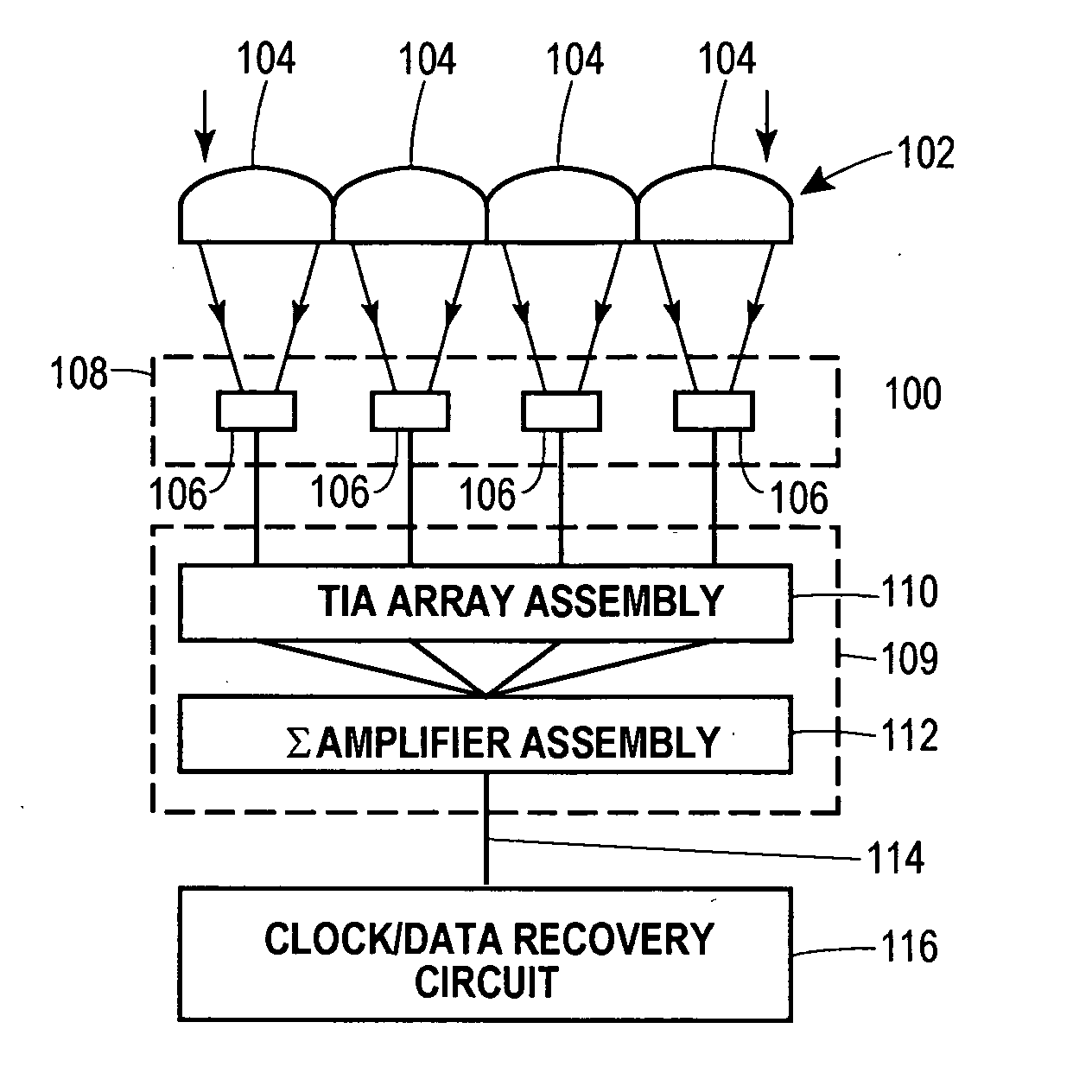
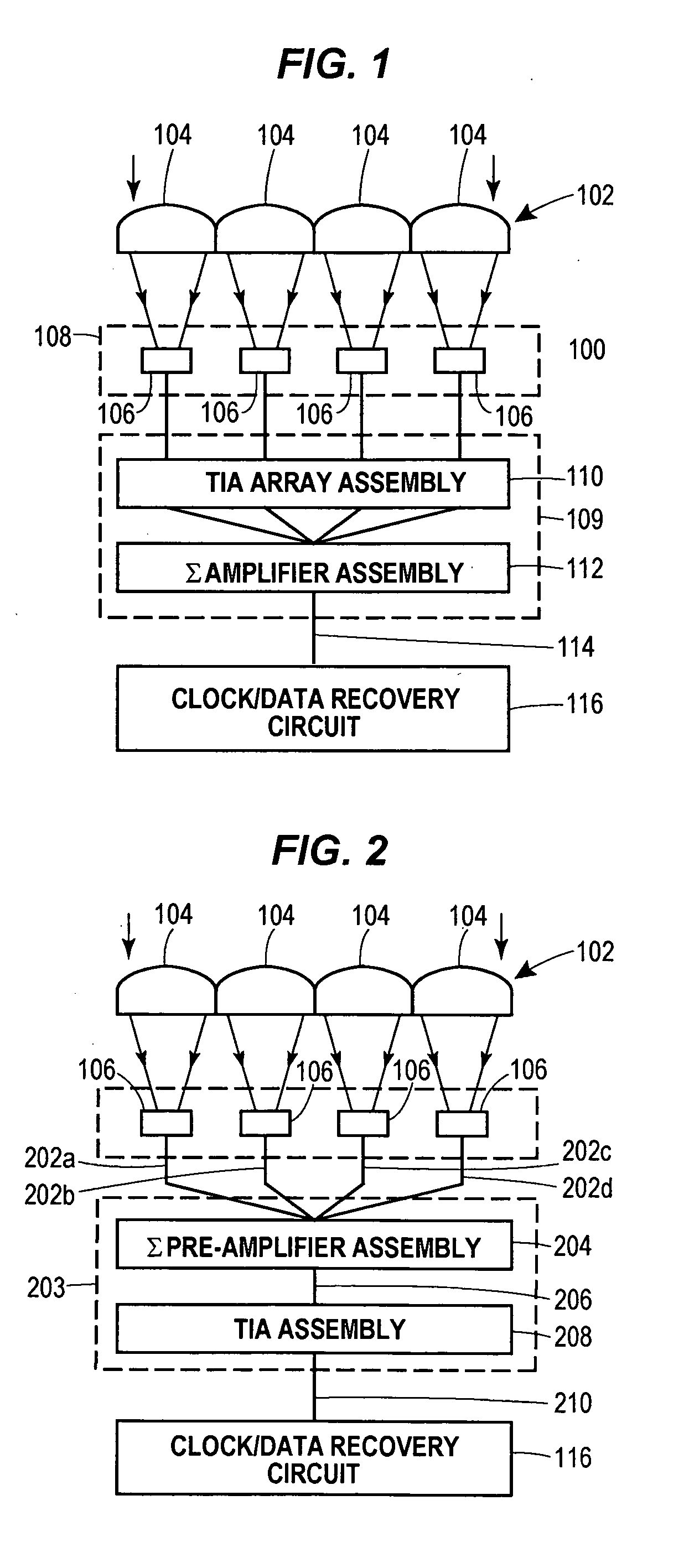
[0020] To detect optical radiation like laser signals, an optical device may have a focal plane assembly (FPA) able to collect the optical energy and direct that energy to an optoelectronic converter, such as a photodetector array. The electrical signals from the photodetector array may then be applied to amplifiers and analog or digital summing elements to produce a rendition of the original laser signal captured by the FPA. FIGS. 1 and 2 illustrate two different configurations of optical devices that may be used in such high data rate optical communication systems.

[0021]FIG. 1 illustrates an optical device 100 that may be used to collect and convert optical signals having data rates of approximately 1 Gbit / s or higher, and in some examples approximately 10 Gbit / s or higher. The device 100 may be used to collect optical energy having a frequency of typically between approximately 1 GHz and 50 GHz, for example.

[0022] The device 100 includes an FPA in the form of a lenslet array 10...


PUM


Abstract

An assembly is provided that may be used in high data rate optical communications, such as free-space communication systems. The assembly may include a main optical receiver element and a lenslet array or other optical element disposed near the focal plane that collects an optical signal and focuses that signal as a series of optical signal portions onto a photodetector array, formed of a series of InGaAs photodiodes, for example. The electrical signals from the photodetectors may be amplified using high bandwidth transimpedance amplifiers connected to a summing amplifier or circuit that produces a summed electrical signal. Alternatively, the electrical signals may be summed initially and then amplified via a transimpedance amplifier. The assembly may be used in remote optical communication systems, including free-space laser communication environments, to convert optical signals up to or above 1 Gbit/s or higher data rates into electrical signals at 1 Gbit/s or higher data rates.

Description

FIELD OF THE INVENTION [0001] The present disclosure generally relates to optical communications and, more particularly, to optical detector arrays that convert an unfocused or blurred spot comprising an optical signal into an electrical signal by summing signals from detectors forming the array. BACKGROUND OF THE RELATED ART [0002] Optical communication is becoming the preferred method for secure, high-bandwidth communications. Fiber-based communication systems, for example, are used in environments where the access points are known and fixed, and free-space communication systems are used in remote applications where access points may vary. For the latter systems, compact, lightweight, field deployable receivers are desired. Yet, the size of existing communications equipment has limited the effectiveness of such devices. [0003] To understand the problems with free-space communications systems, one may look to the environments in which these systems operate. In a standard configurat...

Claims


Application Information

Patent Timeline
Patent Type & Authority Applications(United States)
IPC IPC(8): H01L27/00H04B10/10
CPCH04B10/1121
Inventor WILCKEN, STEPHEN K.SAINT CLAIR, JONATHAN M.
Owner THE BOEING CO
Why Eureka
Try Eureka