

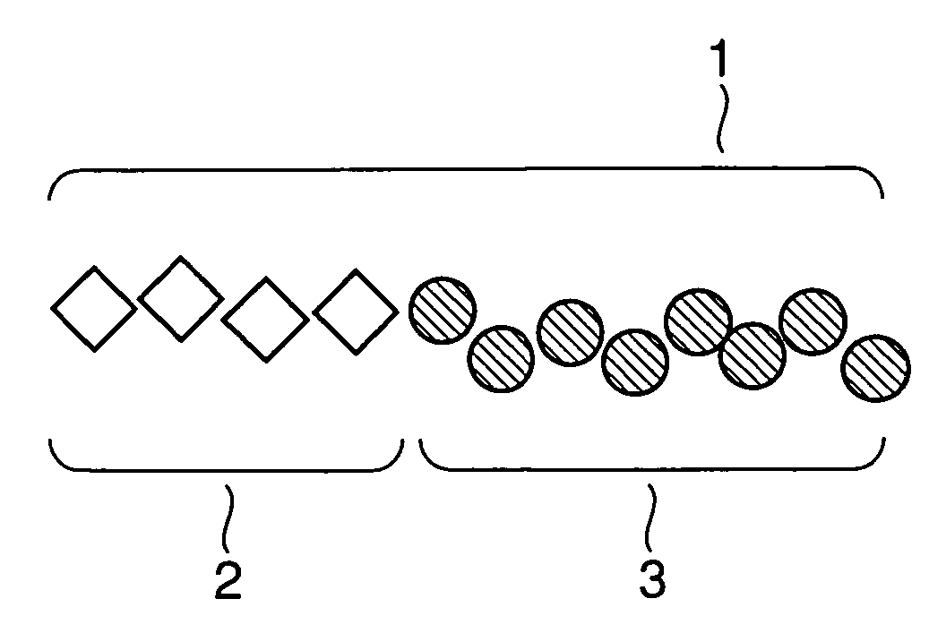
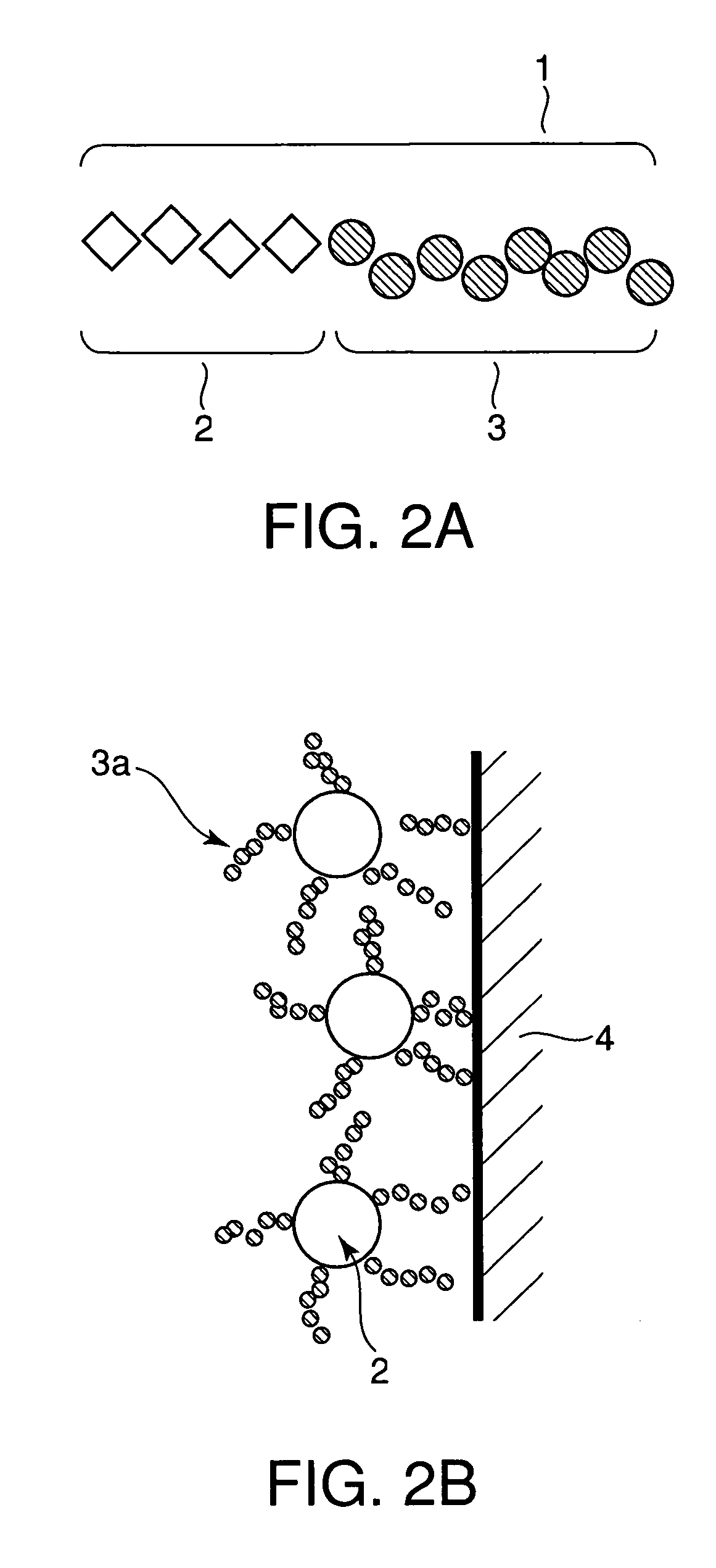
Pattern forming method and method of processing a structure by use of same
a technology of patterning and forming method, which is applied in the direction of superimposed coating process, resistive material coating, liquid/solution decomposition chemical coating, etc., can solve the cost requirement of the lithography process in the manufacturing process is higher, and the problem of not solving the serious problem of reducing patterning throughput remains
- Summary
- Abstract
- Description
- Claims
- Application Information
AI Technical Summary
Benefits of technology
Problems solved by technology
Method used
Image

Examples
example 1
[0038] In Example 1, groove structure is formed by the use of photolithography. A diblock copolymer used as the block copolymer having the mesogen group has 30% by weight of a polyethylene oxide block A and 70% by weight of a block B expressed by the following formula. First, L / S having a groove width W of 300 nm, a groove depth D of 20 nm and a pitch of 500 nm is formed on a resist film of a film thickness of 20 nm by photolithography, which is then spin-coated with a toluene solution of the aforementioned diblock copolymer. Dyeing is performed to facilitate observation of the phase separation structure.
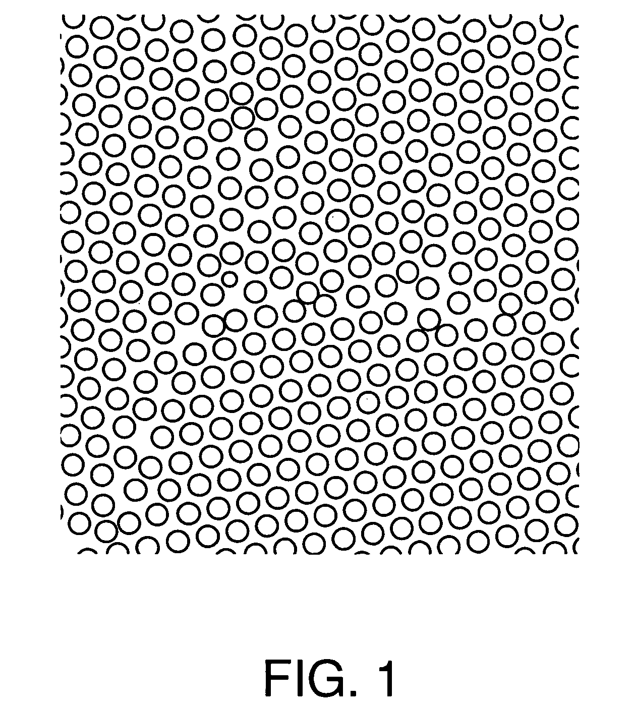
[0039]FIG. 5 shows a TEM image of the patter thus created. FIGS. 6A and 6b show variations in the dot diameters and the array periods A.
example 2
[0042] In Example 2 the case where groove structure is formed by the use of nanoimprint lithography is described. A Ni stamper having line pattern projected in a groove width of 300 nm, a pitch of 500 nm, and a groove depth of 20 nm is fabricated to be used for a novolac resist coated at a film thickness of 50 nm. For fabricating the stamper, the line pattern is written on an electron beam resist on a Si wafer by an electron beam technique. Then, the pattern is transferred at a depth of 20 nm to the Si wafer by RIE using CF4 as an etching gas, and then the remaining resist is removed. After that, Ni spattering is performed on the surface to make it conductive, and then Ni is deposited on the plating. The stamper thus fabricated is pressed against a novolac resist on the sample substrate to transfer the pattern of the stamper to the resist film. When transferring the pattern, the sample is retained at a temperature of 120° C. After the stamper is pressed for about one minute, the sam...
example 3
[0043] In Example 3 the case where the groove depth D of the groove structure is set at D<A / 2 with respect to the array period A of the block copolymer is described. The groove structure is formed by a method using the nanoimprint technique. Regarding the stamper, a Ni stamper having a groove width of 300 nm, a pitch of 500 nm, and a groove depth of 3 nm is fabricated for use. The Ni stamper is fabricated by the same method as that in Example 2. The Ni stamper is pressed against a 20-nm-thick novolac resist film on the sample substrate to transfer the pattern of the stamper to the resist film. At this point, the sample is retained at a temperature of 120° C. After the temperature of the sample substrate is decreased to 80° C. or lower, the stamper and the sample substrate are detached from each other. Then, the novolac resin is hardened by far-ultraviolet radiation. Then, a coating of the same diblock copolymer as that used in Example 1 is applied. The phase separation structure is ...
PUM
| Property | Measurement | Unit |
|---|---|---|
| Temperature | aaaaa | aaaaa |
| Temperature | aaaaa | aaaaa |
| Fraction | aaaaa | aaaaa |
Abstract
Description
Claims
Application Information