Ultra low k plasma enhanced chemical vapor deposition processes using a single bifunctional precursor containing both a SiCOH matrix functionality and organic porogen functionality

a technology of organic porogen and low k plasma, which is applied in chemical vapor deposition coating, transportation and packaging, coatings, etc., can solve the problems of increasing signal delays in ulsi electronic devices, prohibitive mass production use high cost of prior art precursor materials, etc., to achieve better control of film thickness and compositional uniformity, and simplify manufacturing process

Inactive Publication Date: 2006-04-13
GLOBALFOUNDRIES INC
View PDF4 Cites 80 Cited by
  • Summary
  • Abstract
  • Description
  • Claims
  • Application Information

AI Technical Summary

Benefits of technology

[0017] The use of a single organosilicon precursor in a PECVD process enables easier control of the process, better control of film thickness and compositional uniformity and simplifies the manufacturing process. Furthermore, the deposition of a film from a single organosilicon precursor enables better control of the final porosity in the film and a narrower pore size distribution, potentially resulting in better mechanical properties at the same values of dielectric constant. Furthermore, the deposition of a film from a single organosilicon precursor enables better control of the mechanical properties of the final SiCOH dielectric because the bonding in the final film is closely related to the bonding in the single organosilicon precursor with a built-in organic porogen.

Problems solved by technology

This combined effect increases signal delays in ULSI electronic devices.
Most commercially available dielectric materials however are not thermally stable when exposed to temperatures above 300° C. Integration of low k dielectrics in present ULSI chips requires a thermal stability of at least 400° C.
Furthermore, these prior art precursor materials are high cost and prohibitive for use in mass production.
It is commonly found that SiCOH dielectric materials made in the prior art from two or more separate organosilicon and / or porogen precursors are not uniform in atomic and structural composition, both when measured across the substrate diameter, and through the depth of the layer.
The use of 300 mm Si wafers has made this problem of chemical uniformity across the wafer more pronounced.
It is also commonly found that SiCOH dielectric materials made from two or more separate organosilicon and / or porogen precursors exhibit process variation or process instability due to small changes in the flow rate of one of the two precursors, known as drift in the flow rate.

Method used


Image

  • Ultra low k plasma enhanced chemical vapor deposition processes using a single bifunctional precursor containing both a SiCOH matrix functionality and organic porogen functionality
  • Ultra low k plasma enhanced chemical vapor deposition processes using a single bifunctional precursor containing both a SiCOH matrix functionality and organic porogen functionality
  • Ultra low k plasma enhanced chemical vapor deposition processes using a single bifunctional precursor containing both a SiCOH matrix functionality and organic porogen functionality

Examples


Embodiment Construction

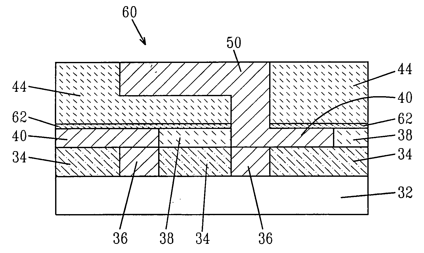
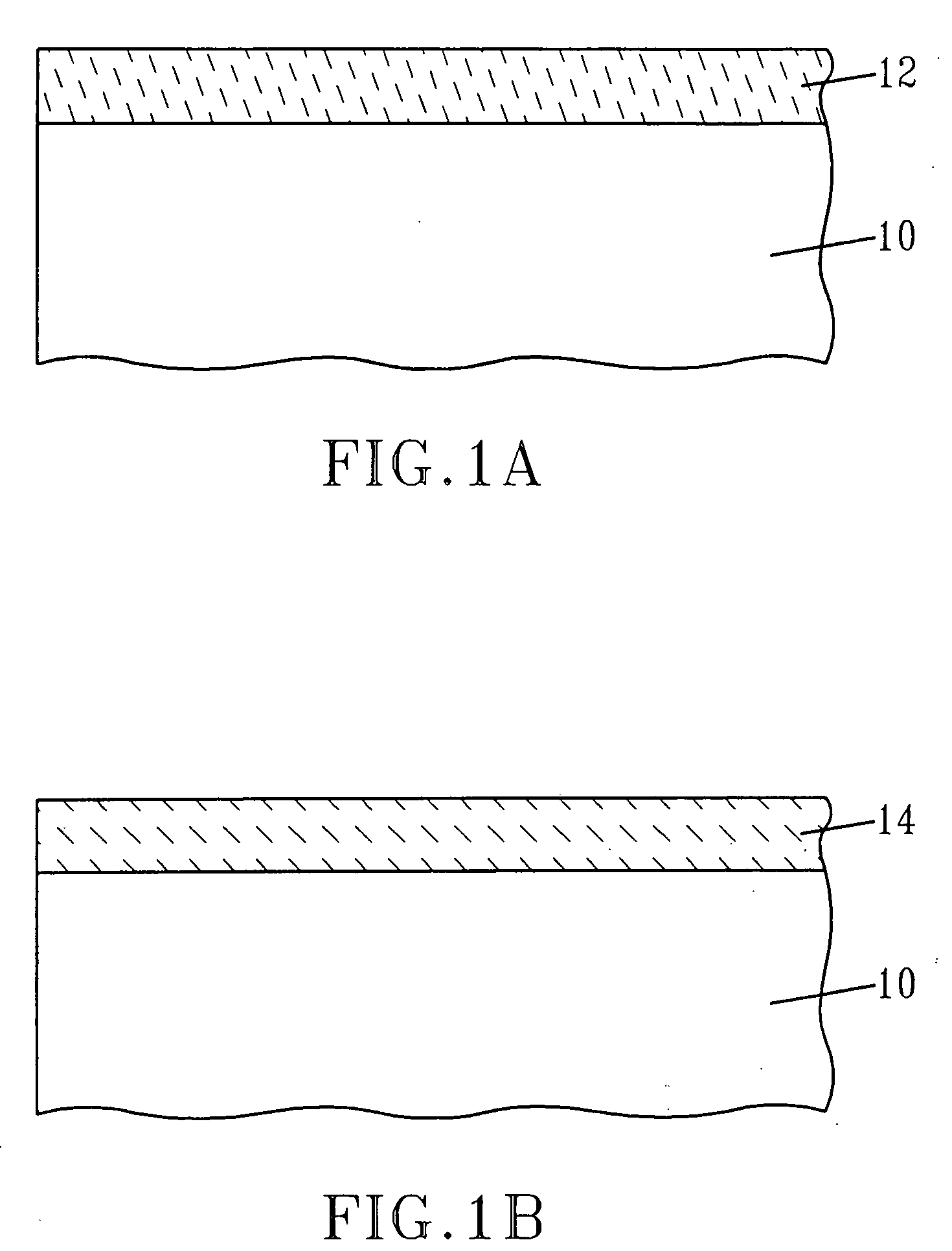
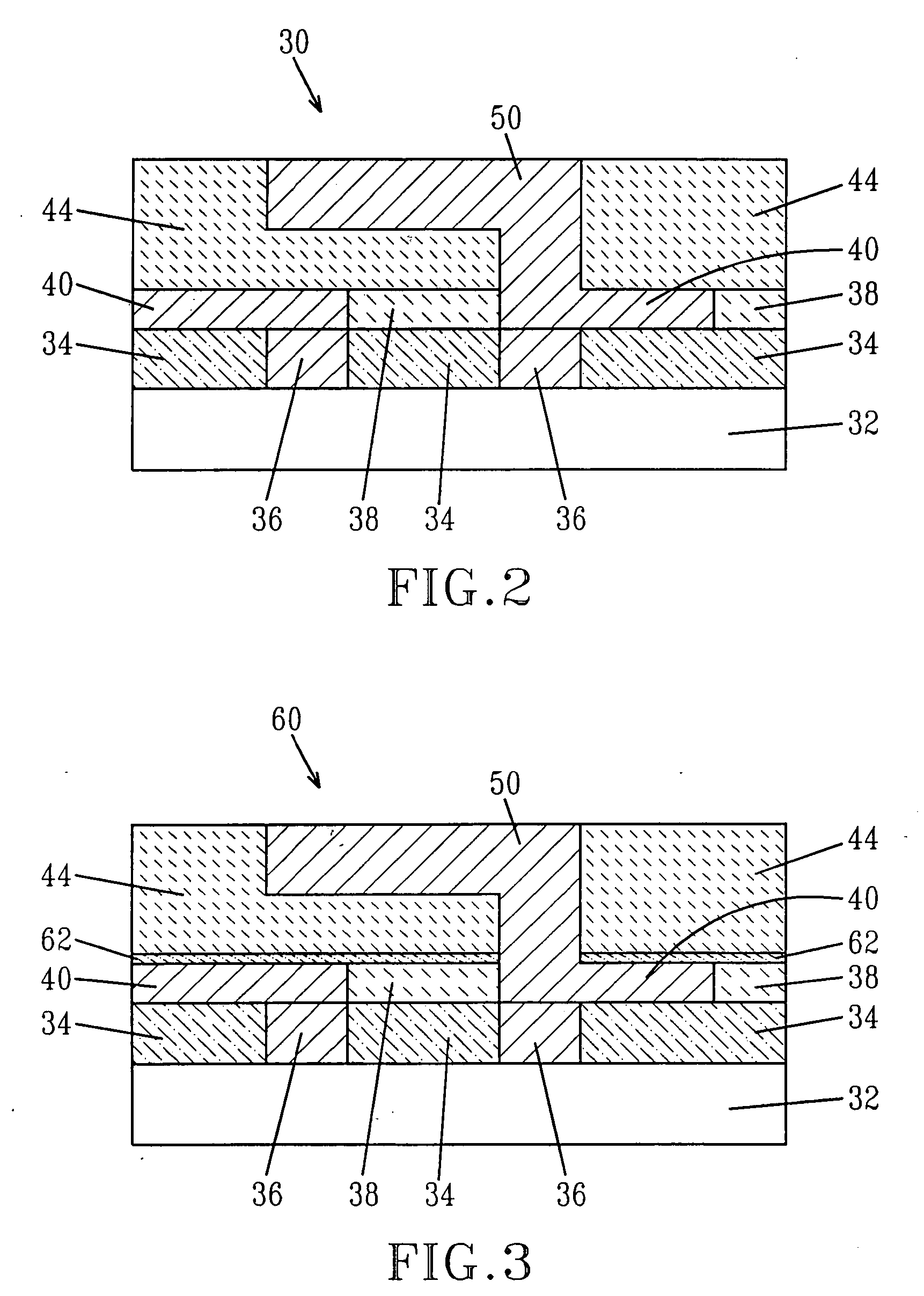
[0030] The present invention, which describes a method of fabricating a SiCOH dielectric material using a single organosilicon precursor containing a built-in organic porogen, a SiCOH dielectric film formed by the inventive method and electronic structures containing the same, will now be described in greater detail.

[0031] In accordance with the method of the present invention, an as deposited dielectric film 12 is formed on a surface of a substrate 10 such as shown, for example, in FIG. 1A. The term “substrate” when used in conjunction with substrate 10 includes, a semiconducting material, an insulating material, a conductive material or any combination thereof, including multilayered structures. Thus, for example, substrate 10 can be a semiconducting material such as Si, SiGe, SiGeC, SiC, GaAs, InAs, InP and other III / V or II / VI compound semiconductors. The semiconductor substrate 10 can also include a layered substrate such as, for example, Si / SiGe, Si / SiC, silicon-on-insulators...


PUM

PropertyMeasurementUnit
dielectric constantaaaaaaaaaa
temperatureaaaaaaaaaa
wavelengthaaaaaaaaaa

Abstract

A method for fabricating a SiCOH dielectric material comprising Si, C, O and H atoms from a single organosilicon precursor with a built-in organic porogen is provided. The single organosilicon precursor with a built-in organic porogen is selected from silane (SiH4) derivatives having the molecular formula SiRR1R2R3, disiloxane derivatives having the molecular formula R4R5R6—Si—O—Si—R7R8R9, and trisiloxane derivatives having the molecular formula R10R11R12—Si—O—Si—R13R14—O—Si—R15R16R17 where R and R1-17 may or may not be identical and are selected from H, alkyl, alkoxy, epoxy, phenyl, vinyl, allyl, alkenyl or alkynyl groups that may be linear, branched, cyclic, polycyclic and may be functionalized with oxygen, nitrogen or fluorine containing substituents. In addition to the method, the present application also provides SiCOH dielectrics made from the inventive method as well as electronic structures that contain the same.

Description

CROSS-REFERENCE TO RELATED APPLICATIONS [0001] The present application is related to co-assigned U.S. Pat. Nos. 6,147,009, 6,312,793, 6,441,491, 6,437,443, 6,541,398, 6,479,110 B2 and 6,497,963, the entire contents of each of the aforementioned U.S. patents are incorporated herein by reference. The present application is also related to the following co-pending and co-assigned U.S. patent application Ser. No. 10 / 174,749, filed Jun. 19, 2002, Ser. No. 10 / 340,000, filed Jan. 23, 2003, Ser. No. 10 / 390,801, filed Mar. 18, 2003, and Ser. No. 10 / 758,724, filed Jan. 16, 2004. The contents of each of the aforementioned U.S. Patent Applications are also incorporated herein by reference in their entirety as well.FIELD OF THE INVENTION [0002] The present invention generally relates to a method of fabricating a dielectric material that has an ultralow dielectric constant (or ultralow k) using a plasma enhanced chemical vapor deposition (PECVD) process in which a single organosilicon precursor c...

Claims


Application Information

Patent Timeline
Patent Type & Authority Applications(United States)
IPC IPC(8): H01L21/31H01L21/469
CPCC23C16/401H01L21/02126H01L21/02216H01L21/02274H01L21/02337H01L21/0234H01L21/02348H01L21/02351H01L21/02362H01L21/3122H01L21/31633H01L21/31695Y10T428/249921
Inventor NGUYEN, SON VANGATES, STEPHEN MACCONNELLNEUMAYER, DEBORAH A.GRILL, ALFRED
Owner GLOBALFOUNDRIES INC
Why Eureka
Try Eureka