Reflective electrode and compound semiconductor light emitting device including the same

a light-emitting device and reflective electrode technology, applied in semiconductor devices, semiconductor lasers, semiconductor lasers, etc., can solve the problems of unstable characteristic of fcled, low light utilization efficiency of p-type electrodes, short life of fcled to which reflective electrodes are applied, etc., to achieve superior ohmic contact characteristics, low light absorption, and high light transmittance

Inactive Publication Date: 2006-04-20
SAMSUNG ELECTRONICS CO LTD
View PDF14 Cites 16 Cited by
  • Summary
  • Abstract
  • Description
  • Claims
  • Application Information

AI Technical Summary

Benefits of technology

[0011] The present invention may provide a reflective electrode having low contact resistance, high reflectance, and improved electric conductivity and a compound semiconductor light emitting device having the same.
[0018] The first electrode layer / third electrode layer, for example Ag / Ni, included in the reflective electrode of the compound semiconductor light emitting device may have a superior ohmic contact characteristic, low light absorbance and high light transmittance. Therefore, a compound semiconductor light emitting device having the reflective electrode according to the present invention may have a low operating voltage, an improved optical power and an improved current-voltage characteristic. The power consumption of the compound semiconductor light emitting device is low, thereby improving light emission efficiency of the compound semiconductor light emitting device.

Problems solved by technology

However, the p-type electrode formed of Ni layer / Au layer is semitransparent, and a TLED to which the p-type electrode is applied has a low light utilization efficiency and low brightness.
Therefore, there are drawbacks in that the FCLED to which the reflective electrode is applied has a short life time and the characteristic of the FCLED is unstable.

Method used


Image

  • Reflective electrode and compound semiconductor light emitting device including the same
  • Reflective electrode and compound semiconductor light emitting device including the same
  • Reflective electrode and compound semiconductor light emitting device including the same

Examples


first embodiment

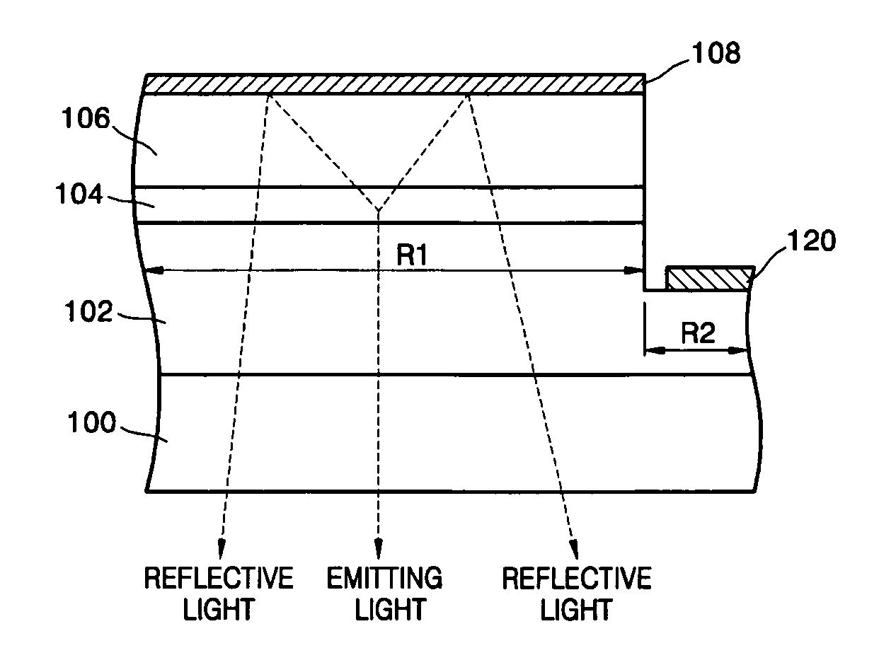
[0027]FIG. 1 is a cross-sectional view illustrating a reflective electrode according to the present invention.

[0028] Referring to FIG. 1, a reflective electrode 22 may be formed on a p-type compound semiconductor layer 20. The reflective electrode 22 according to a first embodiment of the present invention may include sequentially formed a first electrode layer 22a, a third electrode layer 22c and a fourth electrode layer 22d on the p-type compound semiconductor layer 20.

[0029] The first electrode layer 22a may form an ohmic contact with the p-type compound semiconductor layer 20. The first electrode layer 22a may be formed one of Ag and Ag alloy with a thickness of about 0.1 to about 500 nm. Here, the Ag alloy may include at least one material selected from the group consisting of Mg, Zn, Sc, Hf, Zr, Te, Se, Ta, W, Nb, Cu, Si, Ni, Co, Mo, Cr, Mn, Hg, Pr and La.

[0030] The aforementioned Ag and the alloy metal elements may increase the characteristic of ohmic contact of the first e...

second embodiment

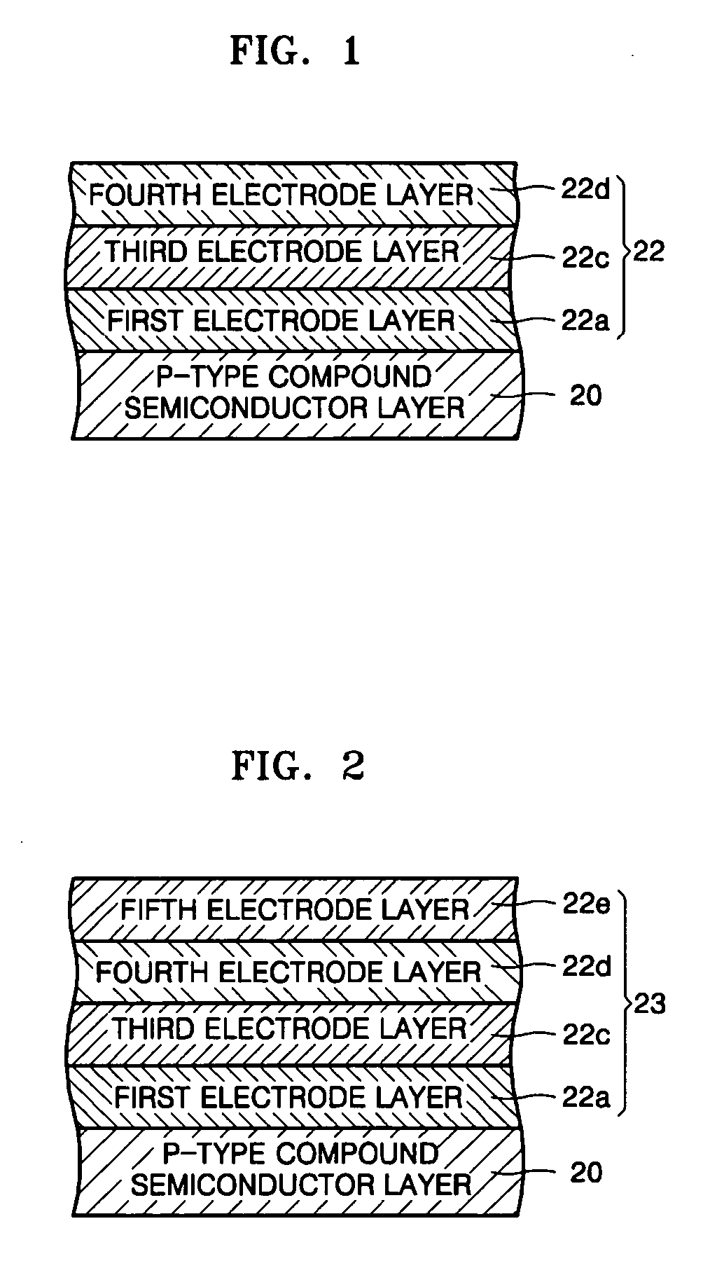
[0038]FIG. 2 is a cross-sectional view illustrating a reflective electrode according to the present invention.

[0039] In the second embodiment of the present invention, mainly the differences from the first embodiment will be described. Like reference numerals refer to like elements in the drawings.

[0040] Referring to FIG. 2, a reflective electrode 23 according to the second embodiment of the present invention may further comprise a fifth electrode layer 22e on the fourth electrode layer 22d of FIG. 1.

[0041] The fifth electrode layer 22e may be formed of a material selected from the group consisting of Cu, Cu / Ru(Cu layer / Ru layer), Cu / Ir(Cu layer / Ir layer), Cu-alloy, Cu-alloy / Ru(Cu-alloy layer / Ru layer) and Cu-alloy / Ir(Cu-alloy layer / Ir layer) with a thickness of about 1 to about 500 nm. The Cu-alloy denotes all alloy materials that include Cu.

[0042] The fifth electrode layer 22e can act as an agglomeration preventing layer for preventing the agglomeration of metal elements on a s...

third embodiment

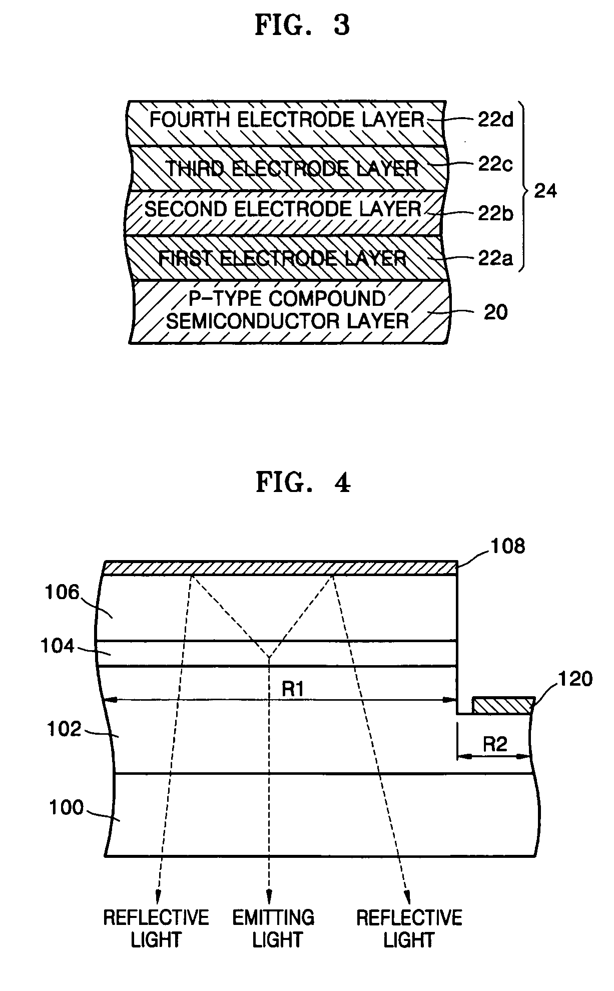
[0047]FIG. 3 is a cross-sectional view illustrating a reflective electrode according to the present invention.

[0048] In the third embodiment of the present invention, mainly the differences from the first embodiment will be described. Like reference numerals refer to like elements in the drawings.

[0049] Referring to FIG. 2, a reflective electrode 24 according to the third embodiment of the present invention further comprises a second electrode layer 22b between the first electrode layer 22a and the third electrode layer 22c in the reflective electrode 22 of FIG. 1.

[0050] The second electrode layer 22b may be formed of Ni or Ni-alloy with a thickness of about 0.1 to about 500 nm.

[0051] The electric conductivity of the reflective electrode 24 may be increased by further including the second electrode layer 22b in the reflective electrode 24.

[0052] The second electrode layer 22b can be formed by an electron beam; an e-beam and thermal evaporator; physical vapor deposition (PVD); ch...


PUM


Abstract

Provided are a reflective electrode and a compound semiconductor light emitting device having the reflective electrode, such as LED or LD is provided. The reflective electrode formed on a p-type compound semiconductor layer of a compound semiconductor light emitting device, comprising a first electrode layer formed one of a Ag and Ag-alloy and forms an ohmic contact with the p-type compound semiconductor layer, a third electrode layer formed of a material selected from the group consisting of Ni, Ni-alloy, Zn, Zn-alloy, Cu, Cu-alloy, Ru, Ir, and Rh on the first electrode layer, and a fourth electrode layer formed of a light reflective material on the third electrode layer.

Description

BACKGROUND OF THE DISCLOSURE [0001] This application claims the priority of Korean Patent Application No. 10-2004-0079963, filed on Oct. 7, 2004, in the Korean Intellectual Property Office, the disclosure of which is incorporated herein in its entirety by reference. [0002] 1. Field of the Disclosure [0003] The disclosure relates to a reflective electrode and a compound semiconductor light emitting device having the same, and more particularly, to a reflective electrode having low contact resistance, high reflectance, and improved electric conductivity and a compound semiconductor light emitting device having the same. [0004] 2. Description of the Related Art [0005] Compound semiconductor light emitting devices can convert an electrical signal to light using a characteristic of a compound semiconductor. Recently, laser light of a semiconductor laser diode, such as a light emitting diode (LED) or a laser diode (LD), is practically used fields, such as optical communications, multiple ...

Claims


Application Information

Patent Timeline
Patent Type & Authority Applications(United States)
IPC IPC(8): H01L33/00H01L33/32H01L33/40
CPCB82Y20/00H01L21/28575H01L33/32H01L33/405H01S5/0425H01S5/1078H01S5/18H01S5/2027H01S5/34333H01S5/04253H01S5/04257
Inventor KIM, MI-YANGKWAK, JOON-SEOP
Owner SAMSUNG ELECTRONICS CO LTD
Why Eureka
Try Eureka