Transistors, integrated circuits, systems, and processes of manufacture with improved work function modulation

a technology of integrated circuits and transistors, applied in the direction of basic electric elements, electrical apparatus, semiconductor devices, etc., can solve the problems of reducing the degree of power dissipation, limiting the extent to which siosub>2 /sub>gate dielectrics can be made thinner, and affecting the effect of power dissipation

Active Publication Date: 2006-04-20
TEXAS INSTR INC
View PDF73 Cites 270 Cited by
  • Summary
  • Abstract
  • Description
  • Claims
  • Application Information

AI Technical Summary

Benefits of technology

[0040]FIG. 8 is a pictorial diagram of a multiple gate field effect transistor improved with silicide-on-doped-barrier gates.

Problems solved by technology

However, currently, the prospect of smaller processes below 0.09 micron (90 nanometers) gate width suggests problems such as 1) increased leakage current that impedes the goal of reduced power dissipation and 2) increased resistances in signal paths that introduce undesirable signal delay that impedes the goal of higher speed and GOPS.
However, there are electrical and physical limitations on the extent to which SiO2 gate dielectrics can be made thinner.
These include gate leakage currents tunneling through the thin gate oxide, difficulty of forming very thin oxide with uniform thickness, and dopant diffusion from the gate through thin gate dielectric into the underlying channel.
Doping diffusion through gate dielectric produces threshold voltage Vt instability, channel mobility degradation and other problems.
Gate polysilicon depletion causes reduction in device performance which leads to poor unscalable devices.
This poly depletion occurs when annealing or other thermal back-end processing of the implanted polysilicon is insufficient to drive the implanted impurities down the entire depth of the polysilicon gate structures or limited by dopant activation level in poly.
A bottom portion of the polysilicon gate contact near the gate dielectric is “depleted” of charges, and acts as an insulator, increases the effective thickness between the effectively-acting gate and the channel and thereby reduces ability to control current flow in the channel.
Simply increasing the implant energy and / or anneal time to combat poly depletion has adverse results, in that the corresponding depths of the concurrently implanted source / drain regions are increased.
Furthermore, because the implant process drives impurities to a variety of depths according to a statistical depth distribution, physical damage to gate dielectric occurs by impact and recoil.
Moreover, alteration and damage not only occur to gate dielectric but also to the channel region by introduction of unintended impurities into both gate dielectric and channel region.
Polysilicon gate technology becomes less attractive as scaling efforts continue.
However, among other problems, the silicidation if carried out over too long a time interval will damage the gate dielectric, and if performed over too short a time interval will not consume all the poly nor pile up sufficient dopant superjacent to the gate dielectric to modify a work function.
Because of variations in real semiconductor device layers and the conditions of practical manufacturing processes, the critical and hard-to-control nature of this silicidation approach portends substantial manufacturing problems and yield uncertainties that translate into higher costs of technology solutions .
The aforementioned problems and uncertainties can be expected to increase as workers consider how to address the challenges posed by sought-after processes with thinner layers of gate dielectric, narrower channel widths, and smaller gate dimensions.
However, this reference seems to require a very large number of steps to complete the gate replacements and various patterning, etching and layer formation steps to provide the various layers of differing materials for the complementary transistors successively and is believed to pose a risk of unavoidably damaging the underlying gate dielectric during poly gate removal or introducing further complication of removing and reforming the gate dielectric itself.
However, among other problems this reference would imply that multiple process steps would be needed to pattern, etch, and lay down the different work function modulation layers with either different materials or different thicknesses, or both, and such complications are believed to pose a risk of difficulty in thickness uniformity control across the wafer.

Method used


Image

  • Transistors, integrated circuits, systems, and processes of manufacture with improved work function modulation
  • Transistors, integrated circuits, systems, and processes of manufacture with improved work function modulation
  • Transistors, integrated circuits, systems, and processes of manufacture with improved work function modulation

Examples


process examples

FOUR CATEGORIES OF PROCESS EXAMPLES

[0119] In summary, among other process and structure embodiments described herein, four categories of alternative process examples contemplated are designated Categories I, II, III and IV.

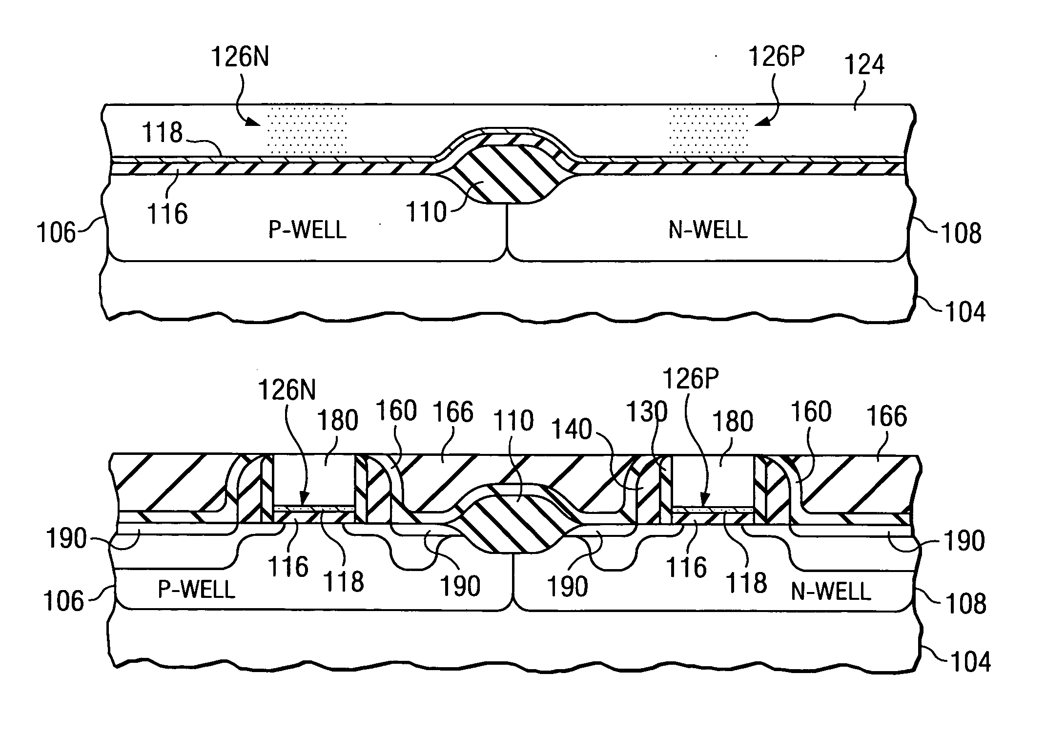
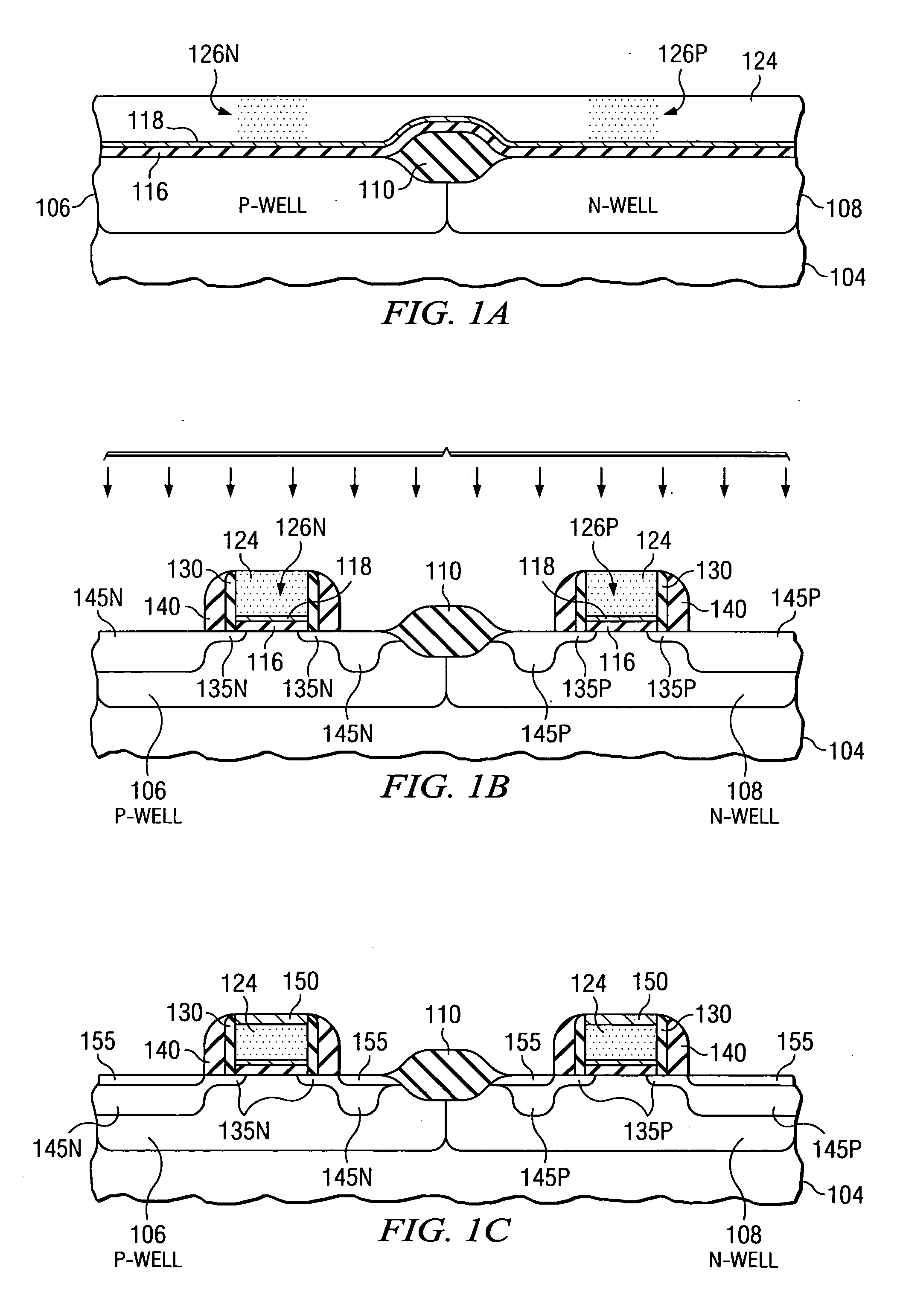
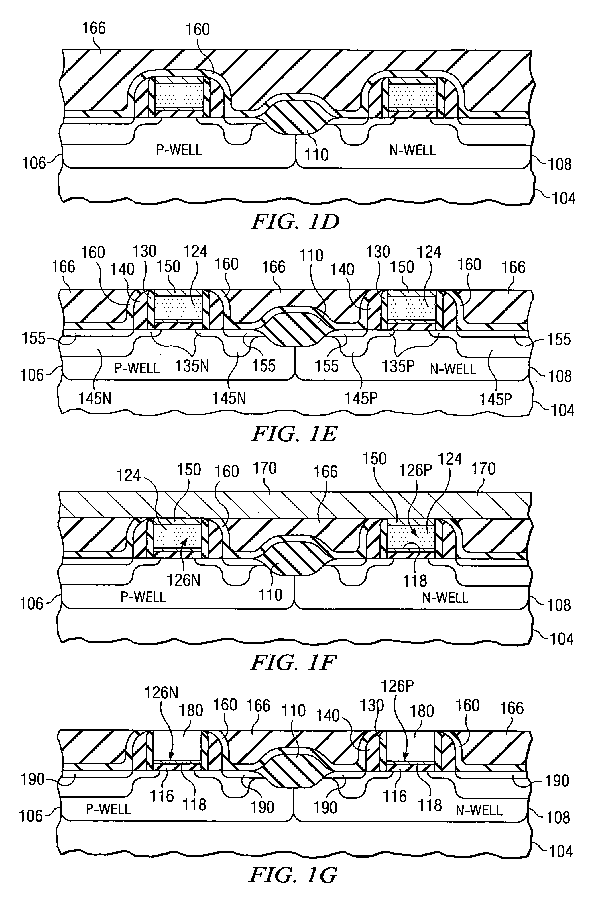
[0120] I. FIGS. 1A-1G and FIG. 2 illustrate structures and process steps in Category I embodiments, which do a prior higher-temperature activation anneal followed by simultaneous silicidation of gate stack and S / D at lower temperature. In a Category 1A, that simultaneous silicidation begins with enough nickel to produce NiSi monosilicide gate and NiSi monosilicide S / D). Silicidation of the gate poly into nickel monosilicide (NiSi) drives gate dopants into the barrier layer thereby advantageously multiplying dopant concentration relative to the poly precursor. In a Category 1B, that simultaneous silicidation begins with about half as much nickel to produce NiSi2 nickel disilicide gate but still produces NiSi monosilicide S / D. Silicidation of the gate poly into nic...


PUM

PropertyMeasurementUnit
widthaaaaaaaaaa
thicknessaaaaaaaaaa
work functionaaaaaaaaaa

Abstract

A process (200) for making integrated circuits with a gate, uses a doped precursor (124, 126N and/or 126P) on barrier material (118) on gate dielectric (116). The process (200) involves totally consuming (271) the doped precursor (124, 126N and/or 126P) thereby driving dopants (126N and/or 126P) from the doped precursor (124) into the barrier material (118). An integrated circuit has a gate dielectric (116), a doped metallic barrier material (118, 126N and/or 126P) on the gate dielectric (116), and metal silicide (180) on the metallic barrier material (118). Other integrated circuits, transistors, systems and processes of manufacture are disclosed.

Description

CROSS-REFERENCE TO RELATED APPLICATIONS [0001] This application is related to provisional U.S. patent application Ser. No. 60 / 620,863, (TI-37388P) filed Oct. 20, 2004, titled “Transistors, Integrated Circuits, Systems, And Processes Of Manufacture With Improved Work Function Modulation,” for which priority under 35 U.S.C. 119(e)(1) is hereby claimed and which is hereby incorporated herein by reference.STATEMENT REGARDING FEDERALLY SPONSORED RESEARCH OR DEVELOPMENT [0002] Not applicable. FIELD OF THE INVENTION [0003] The invention pertains to the fields of transistors, integrated circuits, systems, and processes of their manufacture. BACKGROUND OF THE INVENTION [0004] To mention just one application area, wireless mobile product technology continues to demand more applications performance, less power drain on batteries, and lower integrated circuit cost of manufacture. These demands translate into metrics such as milliwatts of power dissipation per gigahertz (mW / GHz), trillions of op...

Claims


Application Information

Patent Timeline
Patent Type & Authority Applications(United States)
IPC IPC(8): H01L21/04
CPCH01L21/28097H01L21/823835H01L21/823842H01L29/665H01L29/7851
Inventor LIU, KAIPING
Owner TEXAS INSTR INC
Why Eureka
Try Eureka