This helps you quickly interpret patents by identifying the three key elements:
Problems solved by technology
Method used
Benefits of technology
[0024] According to the present invention, as a pre-processing for forming the seed layer for the plating processing, the surface of the resin layer is cut with a cutting cutting tool so as to give the surface of the resin layer suitable roughness. Such processing sufficiently and easily ensures the adhesion between the resin layer and the seed layer. According to the present invention, no excessively deep pores are formed in the surface of the resin layer, as are formed by the desmearing treatment, which permits a micronized pattern to be formed on the resin layer. According to the present invention, the surface roughening processing is made over a large area in a short period of time, which makes it possible to form a micronized pattern to be formed over a large area in a short period of time. Thus, according to the present invention, interconnections, etc. can be easily formed on the resin layer at an extremely small pitch while ensuring high reliability.
[0025] According to the present invention, the dielectric film of the capacitor is formed of a resin sheet, and the surface of the dielectric film is cut with a cutting tool. This processing can suitably adjust the roughness of the surface of the dielectric film of a resin, whereby the adhesion between the dielectric film and the upper electrodes can be sufficiently ensured. According to the present invention, the desmearing treatment is not necessary, and no excessively deep pores are formed in the surface of the dielectric film. Thus, even when the thickness of the dielectric film is made sufficiently small, the insulation between the upper electrodes and the lower electrodes can be sufficiently ensured. The present invention can provide a circuit board having high reliabi
Problems solved by technology
As disclosed in Patent Reference 1, when an object (the resin substrate) for the plating film to be formed on is immersed in an alkaline solution to thereby make the desmearing treatment, deep pores of se
Method used
Image
Click on the blue label to locate the original text in one second.
Reading with bidirectional positioning of images and text.
Examples
Example
A FIRST EMBODIMENT
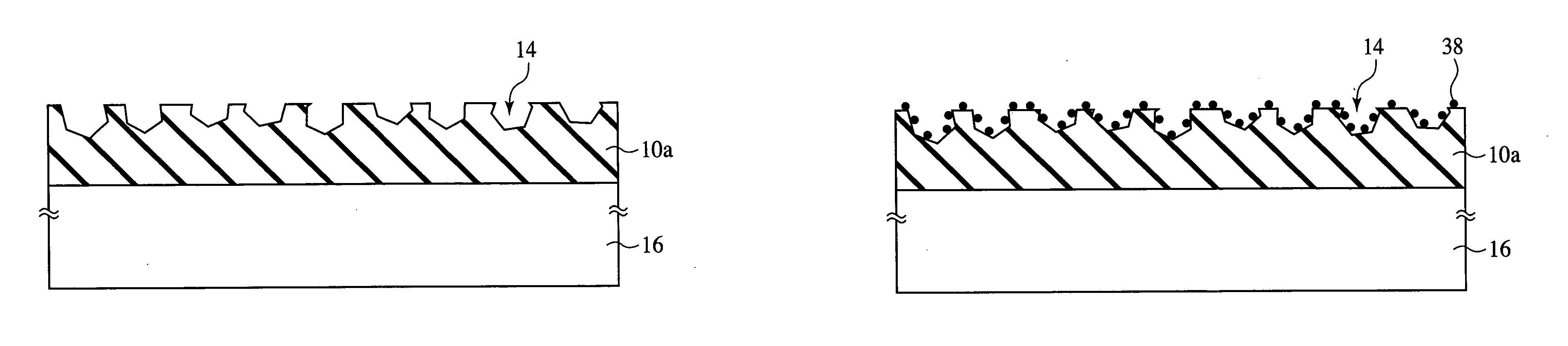
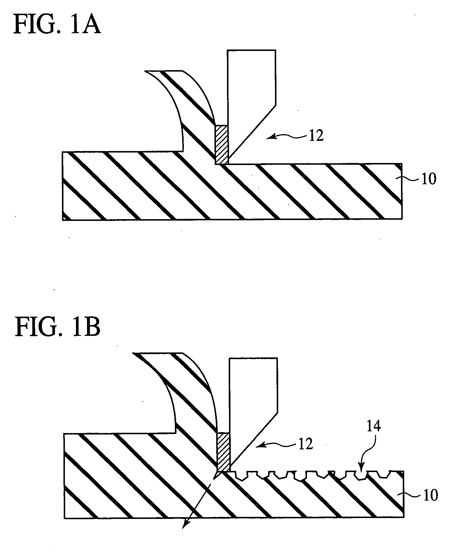
[0079] The plating method according to a first embodiment of the present invention and the semiconductor device fabrication method using the plating method will be explained with reference to FIGS. 2A to 13B and FIG. 29. FIGS. 2A to 12B are sectional views of a semiconductor device in the steps of the semiconductor device fabrication method according to the present embodiment, which illustrate the fabrication method. FIGS. 2A to 6B and 8A to 12B are sectional views, and FIGS. 7A and 7B are plan views.
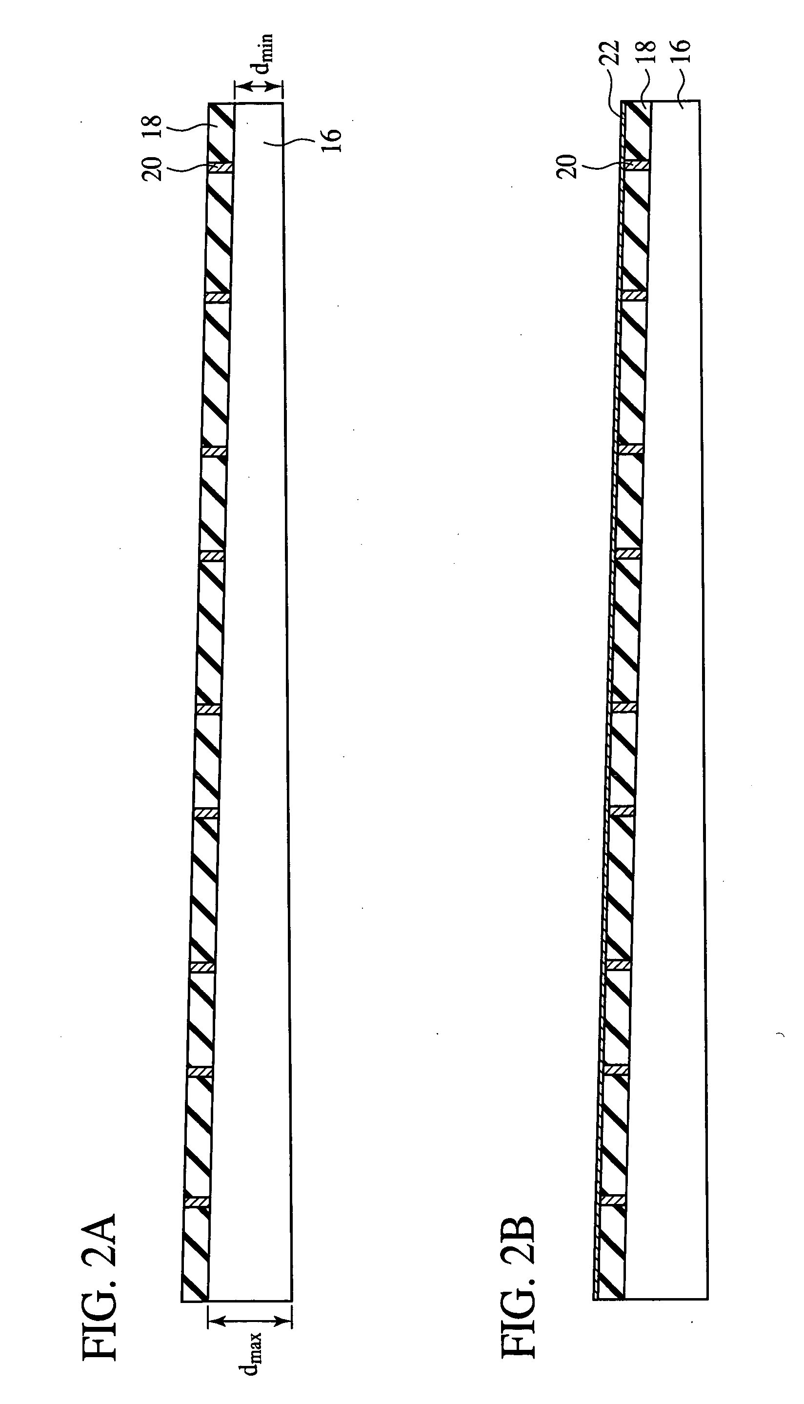
[0080] As illustrated in FIG. 2A, a semiconductor substrate 16 is prepared. The semiconductor substrate 16 is, e.g., a silicon wafer. Transistors (not illustrated), etc. are formed on the semiconductor substrate 16. On the semiconductor substrate 16 with the transistors formed on, an inter-layer insulation film 18 of, e.g., a silicon oxide film is formed. The inter-layer insulation film 18 is formed by, e.g., CVD. A plurality of the inter-layer insulation film 18 are...
Example
A SECOND EMBODIMENT
[0149] The circuit board fabrication method according to a second embodiment of the present invention will be explained with reference to FIGS. 14A to 23. FIGS. 14A to 23 are sectional view of a circuit board in the steps of the circuit board fabrication method, which illustrate the method. The same members of the present embodiment as those of the plating method and the semiconductor device fabrication method according to the first embodiment illustrated in FIGS. 1A to 12B are represented by the same reference numbers not to repeat or to simplify their explanation.
[0150] The circuit board fabrication method according to the present embodiment is characterized mainly in that the dielectric film of capacitors is formed of a resin sheet, and the surface part of the dielectric film of the resin sheet is cut with a cutting tool.
[0151] First, as illustrated in FIG. 14A, a core layer 56 is prepared. The core layer 56 has the following constitution, for example. That ...
Example
A THIRD EMBODIMENT
[0231] The circuit board fabrication method according to a third embodiment of the present invention will be explained with reference to FIGS. 24A to 25B. FIGS. 24A to 25B are sectional views of a circuit board in the steps of the circuit board fabrication method according to a third embodiment of the present invention. The same members of the present embodiments as those of the plating method and the semiconductor device fabrication method or the circuit board fabrication method according to the first or the second embodiment illustrated in FIGS. 1A to 23 are represented by the same reference numbers not to repeat or to simplify their explanation.
[0232] The circuit board fabrication method according to the present embodiment is characterized mainly in that a resistor layer forming resistor is formed of a resin film, and the surface part of the resistor layer is cut with a cutting tool.
[0233] First, the steps up to the step of forming electrodes 82 including the...
PUM
Abstract
The plating method comprises the step of forming a resin layer 10 over a substrate 16; the step of cutting the surface part of the resin layer 10 with a cutting tool 12; the step of forming a seed layer 36 on the resin layer 10 by electroless plating; and the step of forming a plating film 44 on the seed layer 36 by electroplating. Suitable roughness can be give to the surface of the resin layer 10, whereby the adhesion between the seed layer 36 and the resin layer 10 can be sufficiently ensured. Excessively deep pores are not formed in the surface of the resin layer 10, as are by desmearing treatment, whereby a micronized pattern of a photoresist film 40 can be formed on the resin layer 10. Thus, interconnections 44, etc. can be formed over the resin layer 10 at a narrow pitch with high reliability ensured.
Description
CROSS-REFERENCE TO RELATED APPLICATIONS [0001] This application is a continuation-in-part of Ser. No. 11 / 066,481, filed on Feb. 28, 2005. [0002] This application is based upon and claims the benefit of priorities from the prior Japanese Patent Application No. 2004-303345, filed on Oct. 18, 2004, and the prior Japanese Patent Application No. 2005-235229, filed on Aug. 15, 2005, the entire contents of which are incorporated herein by reference.BACKGROUND OF THE INVENTION [0003] The present invention relates to a plating method, and a semiconductor fabrication method and a circuit board fabrication method using the plating method, more specifically, a plating method which can realize high reliability, and a semiconductor device fabrication method and a circuit board fabrication method using the plating method. [0004] In the multi-layer interconnections formed on semiconductor substrates or circuit boards, inter-layer insulation films are required for the electric insulation between the...
Claims
Application Information
Patent Timeline
Application Date:The date an application was filed.
Publication Date:The date a patent or application was officially published.
First Publication Date:The earliest publication date of a patent with the same application number.
Issue Date:Publication date of the patent grant document.
PCT Entry Date:The Entry date of PCT National Phase.
Estimated Expiry Date:The statutory expiry date of a patent right according to the Patent Law, and it is the longest term of protection that the patent right can achieve without the termination of the patent right due to other reasons(Term extension factor has been taken into account ).
Invalid Date:Actual expiry date is based on effective date or publication date of legal transaction data of invalid patent.