Low temperature sin deposition methods

Inactive Publication Date: 2006-04-20
APPLIED MATERIALS INC
View PDF99 Cites 150 Cited by
  • Summary
  • Abstract
  • Description
  • Claims
  • Application Information

AI Technical Summary

Benefits of technology

[0013] The present invention generally provides a method for depositing a layer comprising silicon and nitrogen on a substrate within a processing region. According to an embodiment of the present invention, the method includes the steps of introducing a silicon containing precursor into the processing region, exhausting gases in the processing region including the silicon containing precursor while uniformly, gradually reduc

Problems solved by technology

However, SiI4 is a solid with low volatility making low temperature silicon nitride deposition process difficult.
The high hydrogen content of these materials can be detrimental to device performance by enhancing boron diffusion through the gate dielectric for positive channel metal oxide semiconductor (PMOS) devices and by deviating from stoichiometric film wet etch rates.
When HCDS decomposes, the thic

Method used


Image

  • Low temperature sin deposition methods
  • Low temperature sin deposition methods
  • Low temperature sin deposition methods

Examples


Embodiment Construction

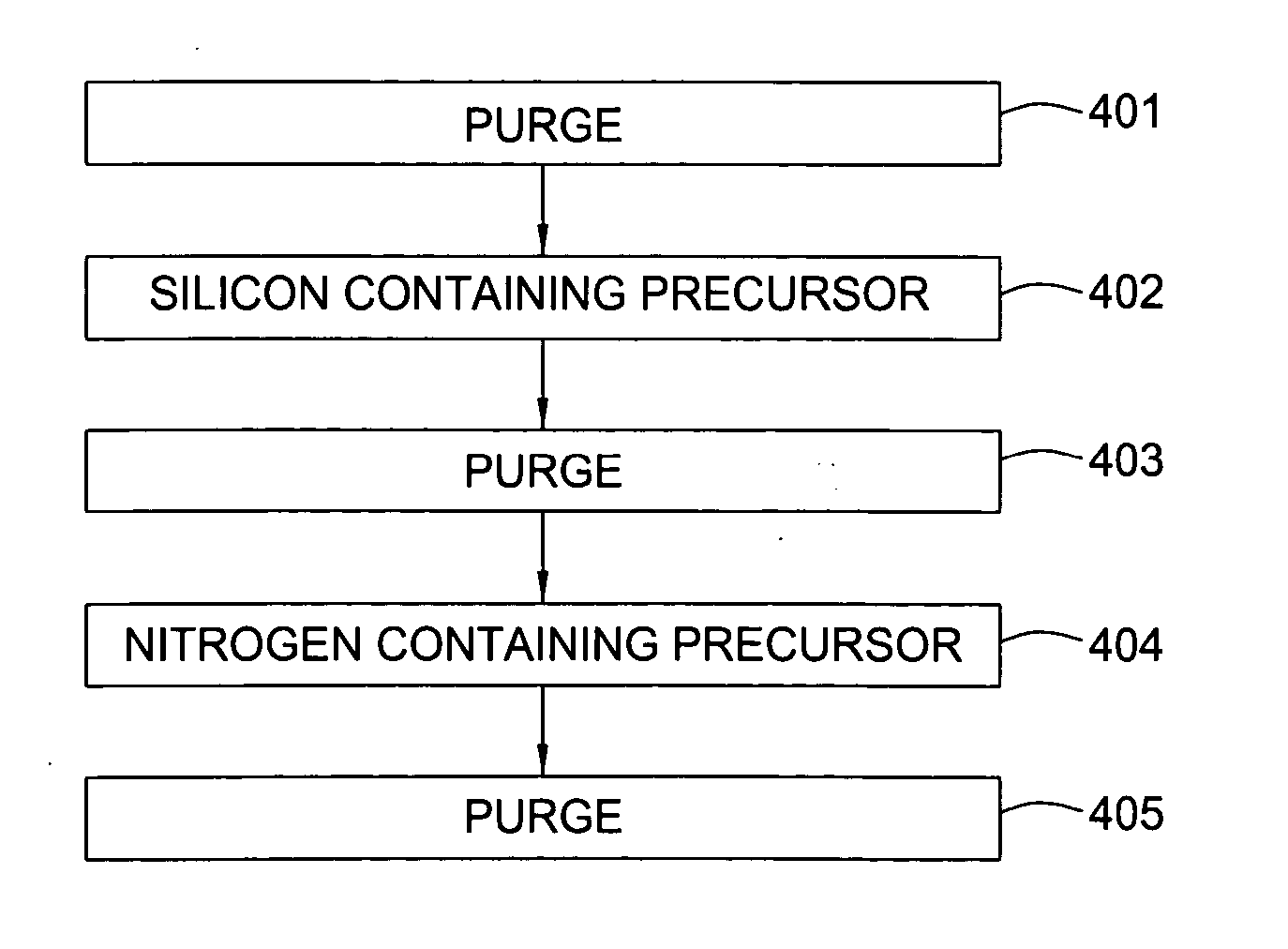
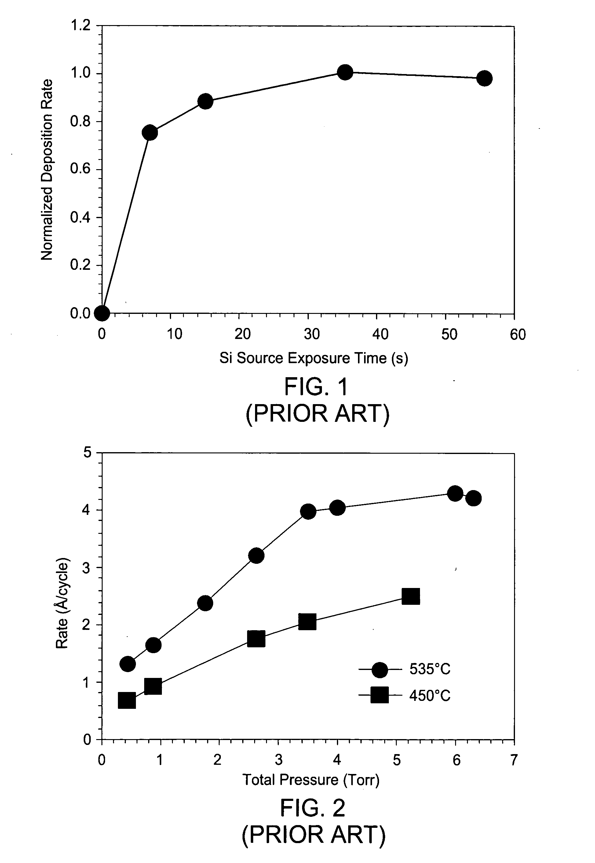
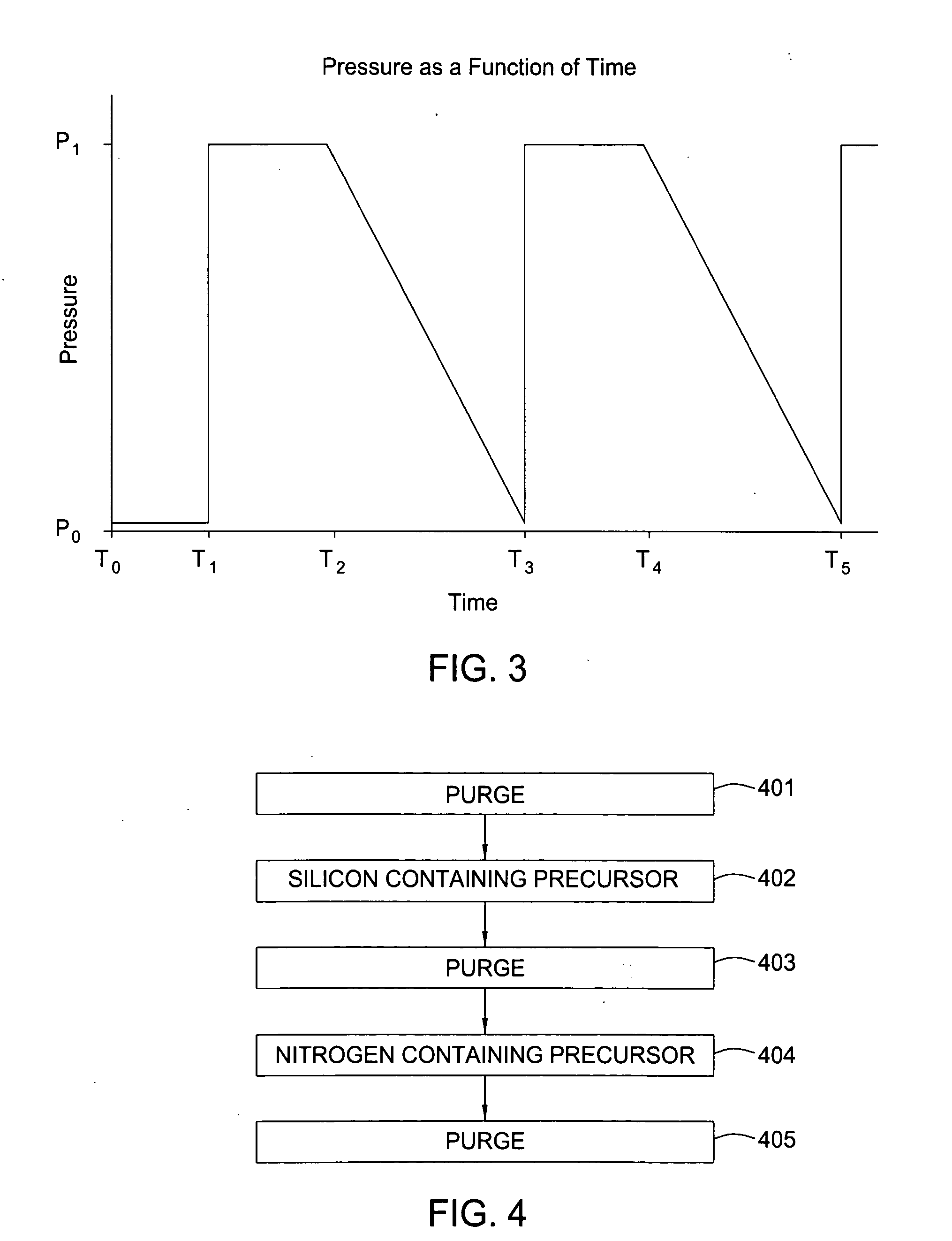
[0021] The present invention provides methods and apparatus for substrate processing including low temperature deposition of silicon nitride films. This detailed description will describe silicon containing precursors, nitrogen containing precursors, and other process gases. Next, process conditions will be described. Finally, experimental results and advantages will be presented. This invention may be performed in a FlexStar™ chamber available from Applied Materials, Inc. of Santa Clara, Calif. or any other chamber configured for substrate processing under conditions specified herein. Detailed hardware information may be found in U.S. Pat. No. 6,352,593, U.S. Pat. No. 6,352,594, U.S. patent application Ser. No. 10 / 216,079, and U.S. patent application Ser. No. 10 / 342,151 which are incorporated by reference herein. Carrier gases for the introduction of the precursor gases include argon and nitrogen. Purge gases for the purge steps in the process include argon and nitrogen.

Silicon C...


PUM

PropertyMeasurementUnit
Temperatureaaaaaaaaaa
Timeaaaaaaaaaa

Abstract

A silicon nitride layer is deposited on a substrate within a processing region by introducing a silicon containing precursor into the processing region, exhausting gases in the processing region including the silicon containing precursor while uniformly, gradually reducing a pressure of the processing region, introducing a nitrogen containing precursor into the processing region, and exhausting gases in the processing region including the nitrogen containing precursor while uniformly, gradually reducing a pressure of the processing region. During the steps of exhausting, the slope of the pressure decrease with respect to time is substantially constant.

Description

BACKGROUND OF THE INVENTION [0001] 1. Field of the Invention [0002] Embodiments of the present invention generally relate to substrate processing. More particularly, the invention relates to chemical vapor deposition processes. [0003] 2. Description of the Related Art [0004] Chemical vapor deposited (CVD) films are used to form layers of materials within integrated circuits. CVD films are used as insulators, diffusion sources, diffusion and implantation masks, spacers, and final passivation layers. The films are often deposited in chambers that are designed with specific heat and mass transfer properties to optimize the deposition of a physically and chemically uniform film across the surface of a substrate. The chambers are often part of a larger integrated tool to manufacture multiple components on the substrate surface. The chambers are designed to process one substrate at a time or to process multiple substrates. [0005] As device geometries shrink to enable faster integrated cir...

Claims


Application Information

Patent Timeline
IPC IPC(8): H01L21/31
CPCC23C16/345C23C16/4412C23C16/45525H01L21/3185H01L21/0228H01L21/02211H01L21/0217C23C16/303C23C16/448H01L21/0262
Inventor PARANJPE, AJIT P.ZHANG, KANGZHANMCDOUGALL, BRENDANVEREB, WAYNEPATTEN, MICHAELGOLDMAN, ALANNAG, SOMNATH
Owner APPLIED MATERIALS INC
Why Eureka
Try Eureka