Ferroelectric film, ferroelectric capacitor, ferroelectric memory, piezoelectric element, semiconductor element, method of manufacturing ferroelectric film, and method of manufacturing ferroelectric capacitor

a manufacturing method and technology of ferroelectric film, applied in the field of ferroelectric capacitors, ferroelectric capacitors, piezoelectric elements, etc., can solve the problems of lack of reliability, difficult to ensure reliability, and inability to provide a ten-year guarantee, and achieve the effect of satisfying characteristics

Inactive Publication Date: 2006-04-27
SEIKO EPSON CORP
View PDF29 Cites 32 Cited by
  • Summary
  • Abstract
  • Description
  • Claims
  • Application Information

AI Technical Summary

Benefits of technology

[0018] The present invention may provide a 1T1C, 2T2C, or simple matrix type of ferroelectric memory including a ferroelectric capacitor having a hysteresis characteristic that can be used in any of a 1T1C, 2T2C, or simple matrix type of ferroelectric memory. The present invention may also provide a ferroelectric film that is suitable for the above-described ferroelectric memory, together with a method of manufacturing the same. The present invention may further provide a piezoelectric element and semiconductor element in which the above-described ferroelectric film is used. The present invention may still further provide a ferroelectric capacitor, a method of manufacture thereof, and a ferroelectric memory in which the ferroelectric capacitor is used, wherein satisfactory characteristics are maintained by a simple process that does not necessitate a barrier film.

Problems solved by technology

Of these, the structure of the 1T type leads to the generation of internal electrical fields which shorten the retention (data preservation) to one month, so it is thought to be impossible to provide a guarantee of ten years, which is generally requested of semiconductors.
For that reason, failures occur in the leakage current characteristic or imprint characteristic (measures of hysteresis distortion), making it difficult to ensure reliability.
PZT tetragonal crystals exhibit a hysteresis characteristic that has the squareness suitable for memory applications, but they lack reliability and cannot be used in practice.
In addition, static imprint testing in which data is written once in either the positive or negative direction and the memory device is heated and held at 100° C. has shown that most of the written data disappears after 24 hours.
These problems are intrinsic to the ionic crystals of PZT and to the Pb and Ti that are constituent elements of PZT, and create the greatest technical problem relating to PZT tetragonal thin film in which large proportions of the constituent elements are Pb and Ti.
This technical problems is great because PZT Perovskite is ionic crystals, and is intrinsic to PZT.
As shown in FIG. 45B, since oxygen ions appear in the vicinity of positive ions in the Brownmillerite type of crystal structure, positive ion defects make it difficult for excessive leakage current to increase.
In addition to the above-described generation of leakage currents, insufficiencies of Pb and Ti and the concomitant insufficiency of O, which are lattice defects, cause spatial charge polarization such as that shown in FIG. 46.
When that happens, reverse electrical fields due to lattice defects are created by the electrical fields of ferroelectric polarization can occur, causing a state in which the bias potential is impeded in the PZT crystals, and hysteresis shift or collapse can occur as a result.
The above problems are intrinsic to PZT and it is considered difficult to analyze these problems in pure PZT, so that up until now it has not been possible to implement suitable characteristics for a memory element made by using tetragonal PZT.
Since the ferroelectric film at this point is mainly formed of oxides, the oxides are reduced by the generated hydrogen during the fabrication process, which has an undesirable effect on the characteristics of the ferroelectric capacitor.

Method used


Image

  • Ferroelectric film, ferroelectric capacitor, ferroelectric memory, piezoelectric element, semiconductor element, method of manufacturing ferroelectric film, and method of manufacturing ferroelectric capacitor
  • Ferroelectric film, ferroelectric capacitor, ferroelectric memory, piezoelectric element, semiconductor element, method of manufacturing ferroelectric film, and method of manufacturing ferroelectric capacitor
  • Ferroelectric film, ferroelectric capacitor, ferroelectric memory, piezoelectric element, semiconductor element, method of manufacturing ferroelectric film, and method of manufacturing ferroelectric capacitor

Examples


first embodiment

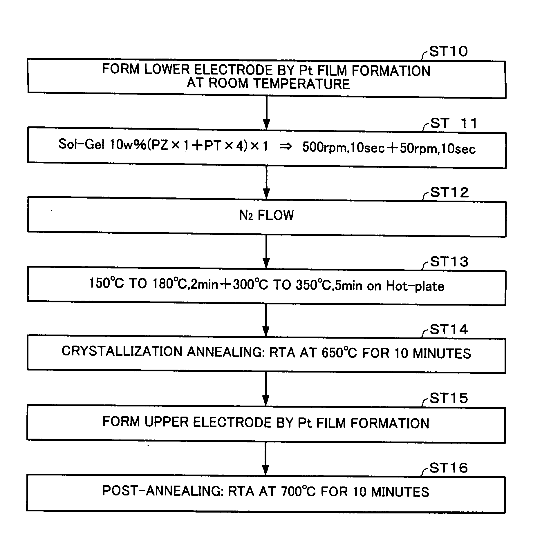
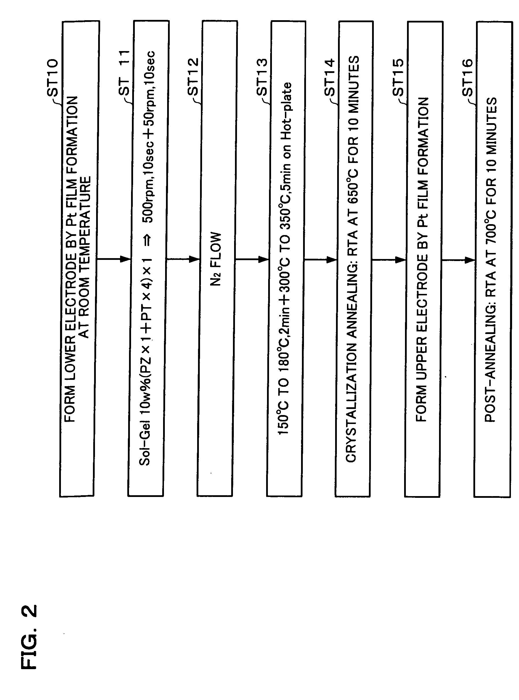
[0121] This embodiment compares the PZTN of the present invention and the PZT of the conventional art. The entire film formation flow shown in FIG. 2 was used.

[0122] Ratios of Pb:Zr:Ti:Nb=1:0.2:0.6:0.2, 1:0.2:0.7:0.1, and 1:0.3:0.65:0.5 were used. In other words, the total quantity of added Nb is 5 to 20 mol %. In this case, 0 to 1% of PbSiO3 is added.

[0123] The surface morphologies of the films in this case are shown in FIGS. 4A to 4C. When the crystallinity of these films were measured by an X-ray diffraction method, the results were as shown in FIGS. 5A to 5C. With the 0% (none) case shown in FIG. 5A, only ordinary paraelectric pyrochlore is obtained, even when the crystallization temperature rises to 800° C. With the 0.5% case shown in FIG. 5B, PZT and the pyrochlore are mixed. With the 1% case shown in FIG. 5C, a single orientated film of PZT (111) is obtained. The crystallinity thereof is also good, of a quality that can not be achieved up to now.

[0124] Next, the crystallin...

second embodiment

[0131] This embodiment is a comparison of the ferroelectric characteristics obtained when the amount of Nb added to the PZTN ferroelectric film was varied to 0, 5, 10, 20, 30, 40 mol %. 5 mol % of PbSiO3 was added to all the testpieces. In addition, methyl succinate was added to the sol-gel solutions for forming the ferroelectric films, includes of raw materials for film formation, to adjust the pH to 6. The entire film formation flow shown in FIG. 2 was used therefor.

[0132] Measured hysteresis characteristics of PZTN ferroelectric films in accordance with this embodiment are shown in FIGS. 17 to 19.

[0133]FIG. 17A shows that when the quantity of added Nb is 0, leaky hysteresis is obtained, whereas FIG. 17B shows that when the quantity of added Nb is 5 mol %, a good hysteresis characteristic with a high level of insulation is obtained.

[0134]FIG. 18A shows that substantially no change is seen in the ferroelectric characteristic until the quantity of added Nb reaches 10 mol %. Even ...

third embodiment

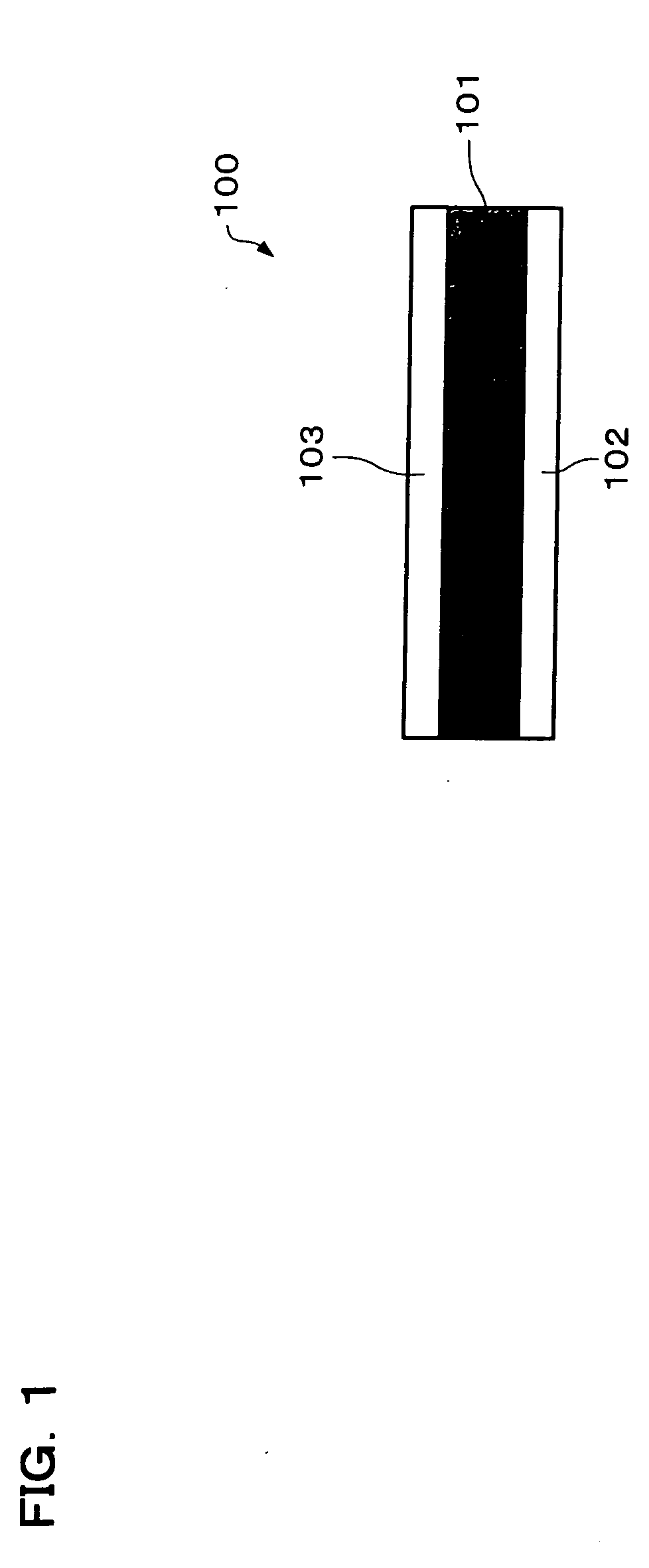
[0145] This embodiment investigates the validity of using a PZTN film from the viewpoint of lattice regularity, when the PZTN film has been formed on a metal film formed of a platinum-group metal such as Pt or Ir as an electrode material for a ferroelectric capacitor that forms a memory cell portion of ferroelectric memory or a piezoelectric actuator that configures an ink ejection nozzle portion of an inkjet printer, by way of example. Platinum-group metals act as underlayer films that determine the crystal orientation of ferroelectric films, and are also useful as electrode materials. However, since the lattice regularities of the two materials are not sufficient, a problem arises concerning the fatigue characteristics of ferroelectric films when applied to elements.

[0146] In this case, the present inventors have developed a technique designed to ameliorate lattice mismatches between a PZT-family ferroelectric film and a platinum-group metal thin film, by incorporating Nb into th...


PUM

PropertyMeasurementUnit
leakage current characteristicsaaaaaaaaaa
crystallization temperatureaaaaaaaaaa

Abstract

A ferroelectric film is formed by an oxide that is described by a general formula AB1-xNbxO3. An A element includes at least Pb, and a B element includes at least one of Zr, Ti, V, W, Hf and Ta. The ferroelectric film includes Nb within the range of: 0.05≦x<1. The ferroelectric film can be used for any of ferroelectric memories of 1T1C, 2T2C and simple matrix types.

Description

CROSS-REFERENCE TO RELATED APPLICATION [0001] This application is a divisional of application Ser. No. 092,800, filed Mar. 8, 2002, which application is incorporated herein by reference in its entirety. [0002] The disclosures of Japanese Patent Application No. 2002-309487, filed on Oct. 24, 2002, Japanese Patent Application No. 2003-76129, filed on Mar. 19, 2003, Japanese Patent Application No. 2003-85791, filed on Mar. 26, 2003, Japanese Patent Application No. 2003-294072 filed on Aug. 18, 2003, and Japanese Patent Application No. 2003-302900 filed on Aug. 27, 2003 are hereby incorporated by reference in their entirety.BACKGROUND OF THE INVENTION [0003] The present invention relates to a ferroelectric film, a ferroelectric capacitor, a ferroelectric memory, a piezoelectric element, a semiconductor element, a method of manufacturing a ferroelectric film, and a method of manufacturing a ferroelectric capacitor. [0004] It has recently become popular to perform research and development...

Claims


Application Information

Patent Timeline
Patent Type & Authority Applications(United States)
IPC IPC(8): B05D5/12B05C5/00C04B35/49B41J2/045B41J2/055B41J2/16C01G25/02C01G33/00C01G35/00C04B35/491H01B1/08H01B3/12H01G4/12H01G4/33H01L21/02H01L21/314H01L21/316H01L21/77H01L21/8246H01L21/84H01L27/10H01L27/105H01L27/115H01L41/08H01L41/09H01L41/18H01L41/187H01L41/318H01L41/39H02N2/00
CPCC01G33/006C01G35/006C01P2002/72C01P2002/77C01P2004/04C01P2004/80C01P2006/40C01P2006/80H01B1/08H01G4/1254H01G4/33H01L21/02197H01L21/02282H01L21/316H01L21/31691H01L27/11502H01L27/11507H01L28/55H01L28/57H01L41/0805H01L41/1876H01L41/318H10N30/1051H10N30/8554H10N30/078H10B53/30H10B53/00H01L27/10H01B3/12
Inventor KIJIMA, TAKESHIHAMADA, YASUAKINATORI, EIJIOHASHI, KOJI
Owner SEIKO EPSON CORP
Why Eureka
Try Eureka