Bond pad structure with stress-buffering layer capping interconnection metal layer

a bond pad and stress buffering technology, applied in the direction of semiconductor devices, electrical equipment, semiconductor/solid-state device details, etc., can solve the problems of affecting the bondability of wire connections, so as to prevent stress-induced damage to the bond pad structure

Inactive Publication Date: 2006-05-04
TAIWAN SEMICON MFG CO LTD
View PDF5 Cites 91 Cited by
  • Summary
  • Abstract
  • Description
  • Claims
  • Application Information

AI Technical Summary

Benefits of technology

[0004] It is an object of the present invention to provide an improved bond pad structure having a stress-buffering layer between a top interconnection level metal layer and a bond pad layer to prevent stress-induced damages to the bond pad structure from wafer acceptance test (WAT) and packaging impacts.

Problems solved by technology

Large mechanical stresses inherent in bonding operations, however, easily damage smaller bonding pads.
When an IC chip is under a wafer accept test (WAT), such as a wafer probing test or the like, a probe pin may damage the soft surface of the aluminum pad, and thereby the underlying copper layer is exposed to air and may be corroded.
The corroded pads caused by this type of pad voids degrade the bondability of wire connection.
The crack may extend into the interior of the IMD layer surrounding the top level copper layer, causing corrosion and layer-open problems.
This also causes the aluminum pad to peel from the top level copper layer, thus the pad-open problem causes the wire to lose contact with the aluminum pad, decreasing bonding reliability.
Additionally, the pitch and size of the bonding pad cannot be further shrunk as the bonding pad is susceptible to damage from the mechanical stress, thus limiting chip size reduction in next generation technologies.

Method used


Image

  • Bond pad structure with stress-buffering layer capping interconnection metal layer
  • Bond pad structure with stress-buffering layer capping interconnection metal layer
  • Bond pad structure with stress-buffering layer capping interconnection metal layer

Examples


Embodiment Construction

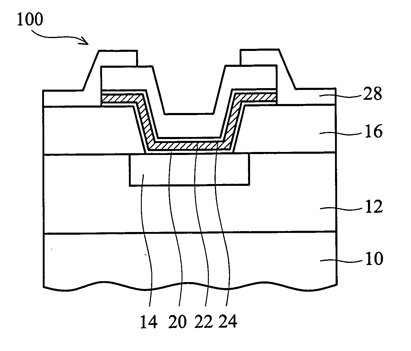
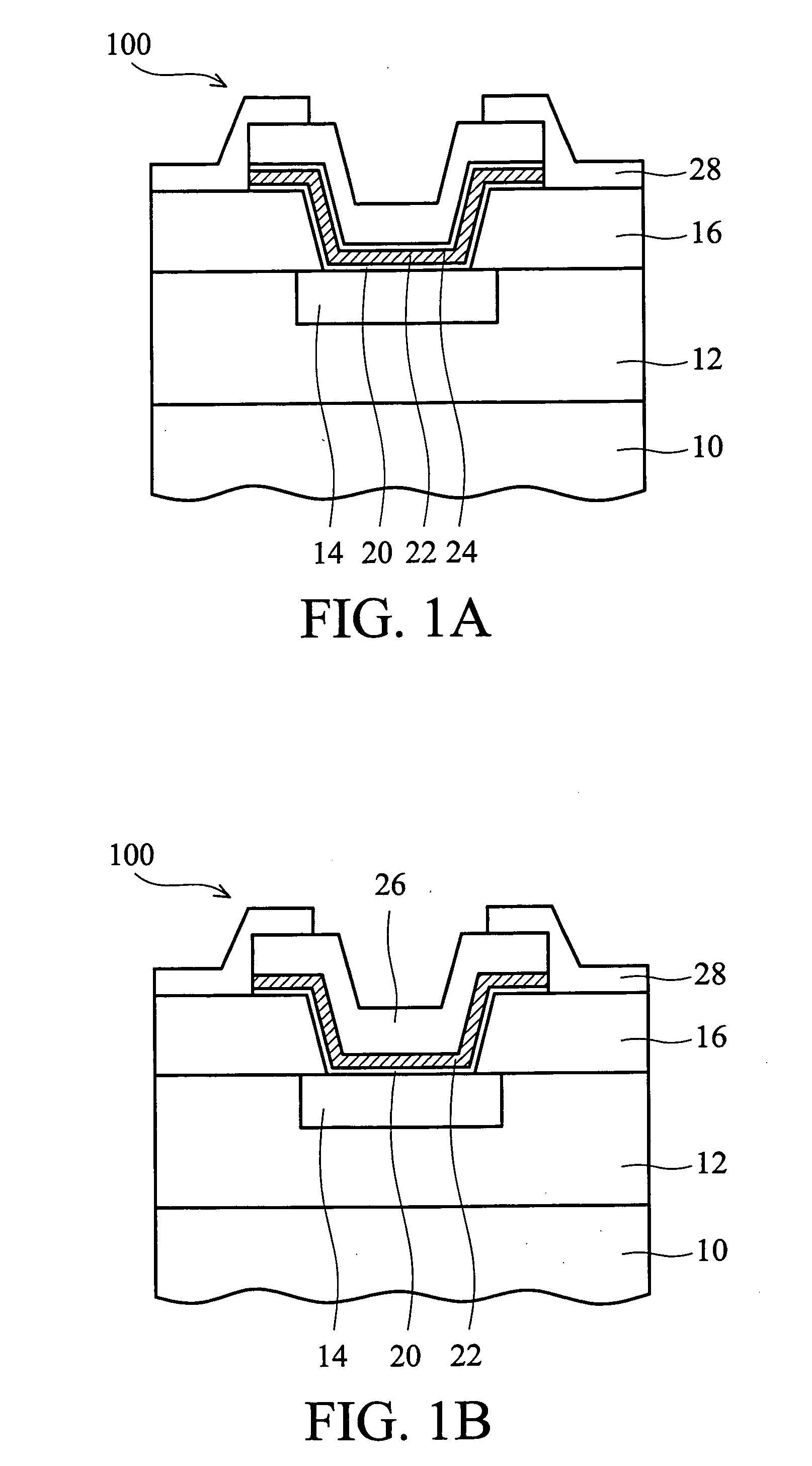
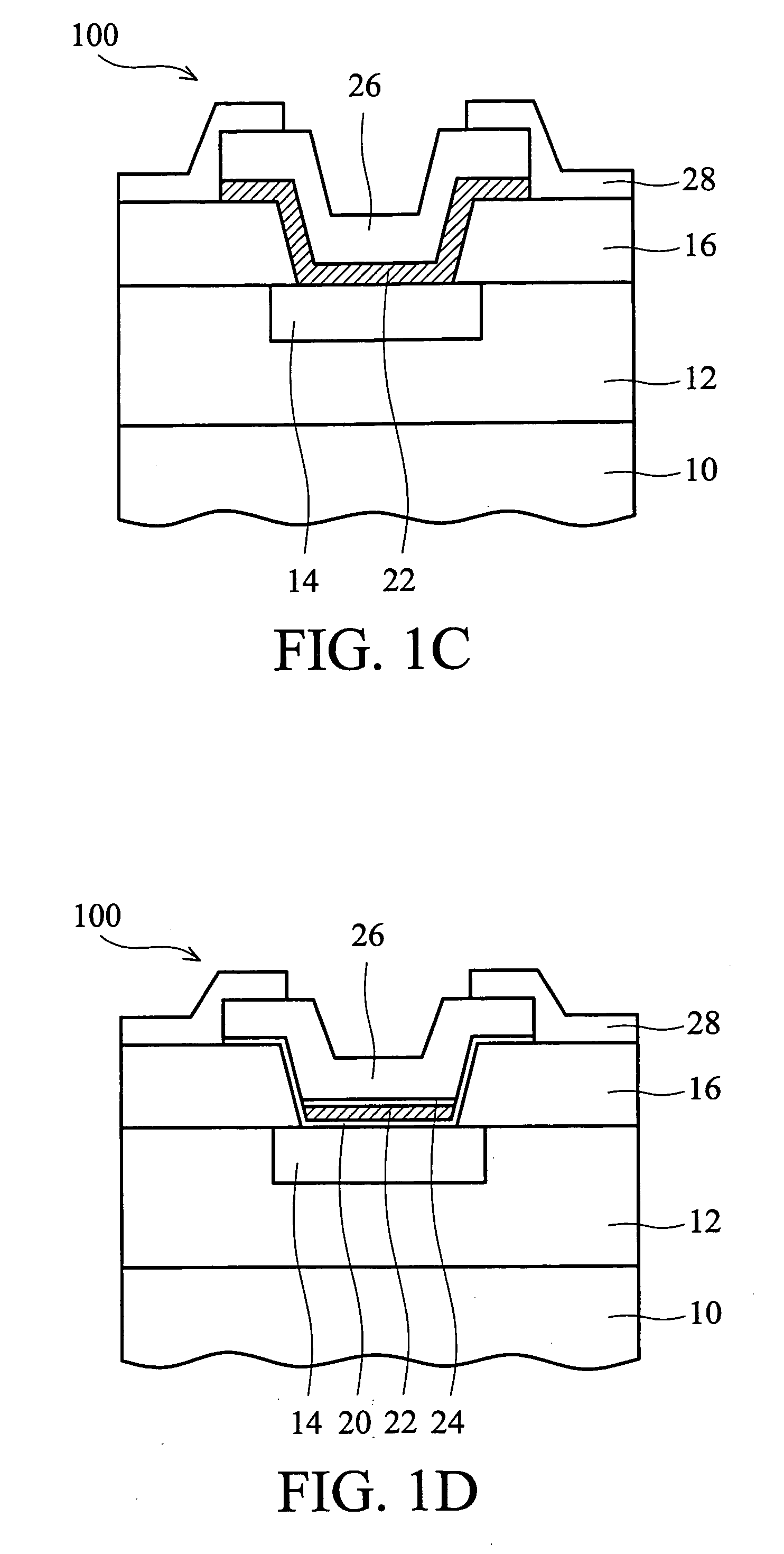
[0019] The present invention provides an improved bond pad structure for an integrated circuit chip. An embodiment of the present invention provides a bond pad structure having a stress-buffering layer between a top interconnection level metal layer and a bond pad layer to prevent stress-induced damages to the bond pad structure from WAT (e.g., wafer probing) and packaging impacts (e.g., applied forces and induced stresses in wire bonding, flip chip or other packaging technologies). The stress-buffering layer is preferably a conductive material having a specific property selected from the group consisting of Young's modulus, hardness, strength and toughness, greater than that of at least one of the top interconnection level metal layer and the bond pad layer. One embodiment of the present invention provides a bond pad structure having a stress-buffering layer between a terminal contact region of a top interconnection level copper-based layer and an aluminum-based bond pad layer on a...


PUM


Abstract

A bond pad structure for an integrated circuit chip has a stress-buffering layer between a top interconnection level metal layer and a bond pad layer to prevent damages to the bond pad structure from wafer probing and packaging impacts. The stress-buffering layer is a conductive material having a property selected from the group consisting of Young's modulus, hardness, strength and toughness greater than the top interconnection level metal layer or the bond pad layer. For improving adhesion and bonding strength, the lower portion of the stress-buffering layer may be modified as various forms of a ring, a mesh or interlocking-grid structures embedded in a passivation layer, alternatively, the stress-buffering layer may has openings filled with the bond pad layer.

Description

FIELD OF THE INVENTION [0001] The present invention relates to bond pad structures, and particularly to a bond pad structure with a stress-buffering layer capping interconnection metal layers for preventing stress induced failure from WAT (wafer accept test) and packaging impacts. BACKGROUND OF THE INVENTION [0002] Bonding pads are interfaces between integrated circuits contained in semiconductor chips and a device package. Each bonding pad is connected to one or more contact pads on an IC-mounting surface of the device package through wire bonding, tape automated bonding, or flip chip technologies. Copper exhibits higher conductivity and greater mechanical integrity, and therefore becomes the material of choice for interconnection wires, contacts and bond pads in future generations. An insulating material that possesses a dielectric constant as low as possible, such as a dielectric constant (k) below the dielectric constant of about 3.9 of silicon dioxide, has been used in copper b...

Claims


Application Information

Patent Timeline
Patent Type & Authority Applications(United States)
IPC IPC(8): H01L23/48H01L23/52H01L29/40
CPCH01L24/05H01L24/45H01L24/48H01L2224/02166H01L2224/0401H01L2224/04042H01L2224/05009H01L2224/05083H01L2224/05093H01L2224/05095H01L2224/05096H01L2224/05147H01L2224/05157H01L2224/05166H01L2224/05171H01L2224/05181H01L2224/05184H01L2224/05187H01L2224/05624H01L2224/45124H01L2224/45144H01L2224/45147H01L2224/48463H01L2924/01004H01L2924/01005H01L2924/01006H01L2924/01012H01L2924/01013H01L2924/01014H01L2924/01015H01L2924/0102H01L2924/01022H01L2924/01025H01L2924/01028H01L2924/01029H01L2924/0103H01L2924/01032H01L2924/01033H01L2924/01038H01L2924/0104H01L2924/01046H01L2924/01047H01L2924/01049H01L2924/0105H01L2924/01058H01L2924/01073H01L2924/01074H01L2924/01078H01L2924/01079H01L2924/01082H01L2924/04941H01L2924/04953H01L2924/0496H01L2924/05042H01L2924/10329H01L2924/14H01L2924/19041H01L2924/19042H01L2924/19043H01L2924/00014H01L2924/01077H01L2924/01019H01L2924/01024H01L2224/48799H01L2924/00H01L2224/48624H01L2224/48824H01L2224/48724H01L2224/02125H01L2924/00012H01L2224/05576H01L2224/05076H01L2224/02126
Inventor HUANG, TAI-CHUNYAO, CHIH-HSIANGWAN, WEN-KAI
Owner TAIWAN SEMICON MFG CO LTD
Why Eureka
Try Eureka