

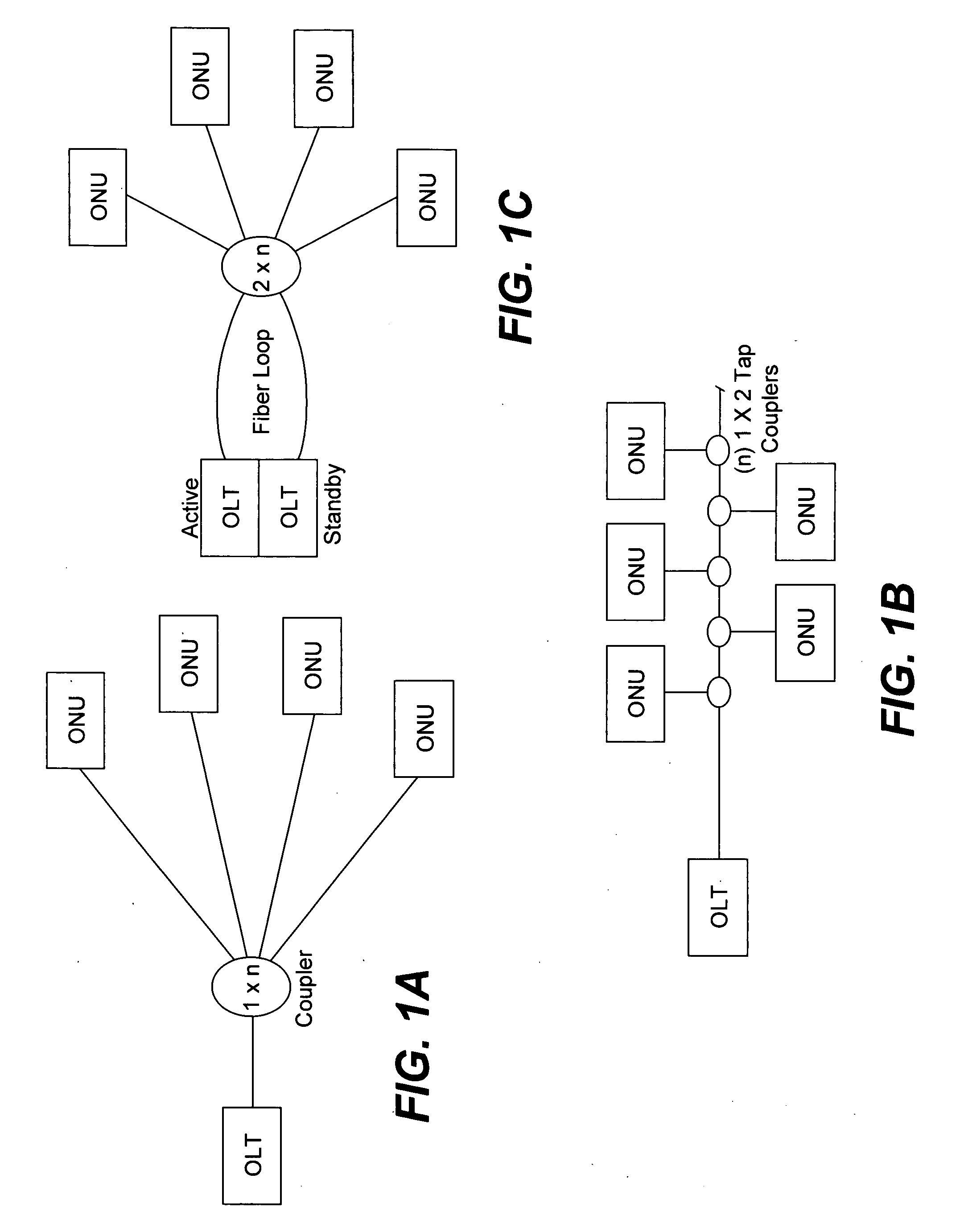
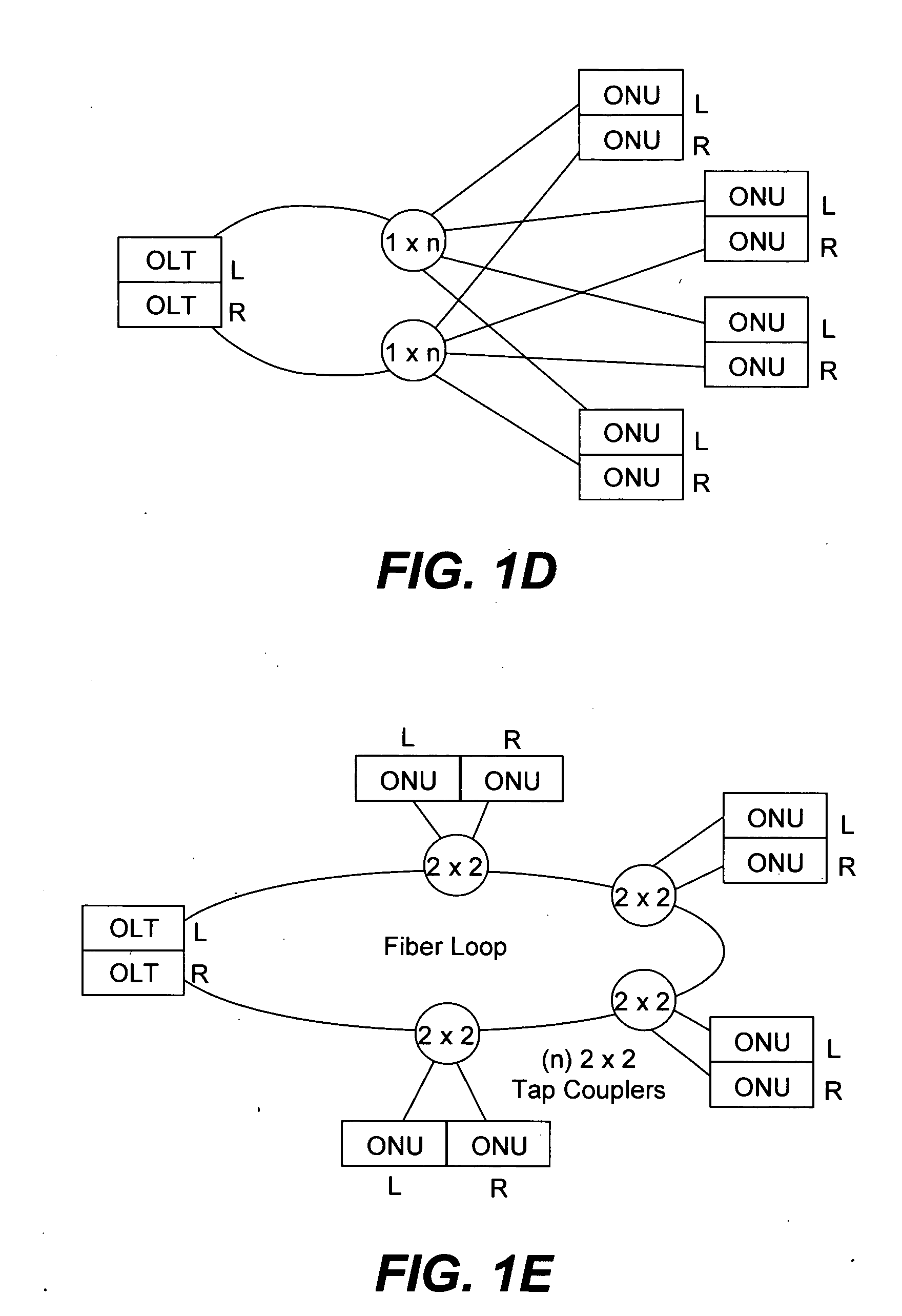
Photonic integrated circuit (PIC) transceivers for an optical line terminal (OLT) and an optical network unit (ONU) in passive optical networks (PONs)
a photonic integrated circuit and optical line terminal technology, applied in electromagnetic transceivers, wavelength-division multiplex systems, electrical apparatus, etc., can solve the problems of providing a significant cost difference from the deployment of aons and an expensive last mil
- Summary
- Abstract
- Description
- Claims
- Application Information
AI Technical Summary
Benefits of technology
Problems solved by technology
Method used
Image

Examples
first embodiment
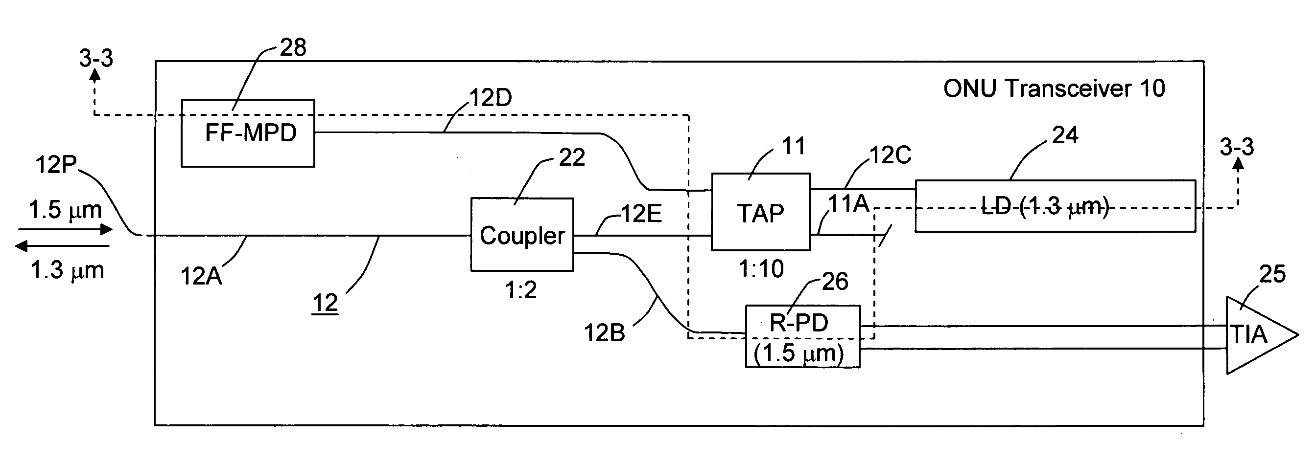
[0031] Reference is now made to FIGS. 2 and 3 illustrating this invention. The photonic integrated circuit (PIC) shown is an ONU transceiver chip 10 comprising a large or “fat” mode waveguide 12 including input / output waveguide 12A to an optical splitting coupler 22 which may be a multi-mode (MM) type coupler such as, for example, a multimode interference (MMI) coupler, a star coupler or a directional coupler. The principal construction and operation of such wavelength sensitive couplers, such as in the case of an MMI coupler, are disclosed in U.S. Pat. No. 5,689,597, U.S. patent application 2003 / 0174960, U.S. Pat. No. 4,484,794 or U.S. Pat. No. 6,580,844, all of which are incorporated herein by their reference. See also, for example, the multimode coupler illustrated in FIG. 5(a) of U.S. Pat. No. 6,580,844. Coupler 22 may also be a Y-branch coupler.
[0032] As previously indicated, the multi-mode interference principal is based on self-imaging where the input signal to the MM coupler...
third embodiment
[0042]FIGS. 7 and 8 illustrate this invention for an ONU transceiver. Transceiver 70 is similar in basic fundamentals to the transceiver shown in U.S. Pat. No. 5,031,188 to Koch et al. except that the construction of transceiver 70 here is importantly different. Transceiver 70 includes an inline electro-optic element train, starting at input / output waveguide 72, a 1.3 μm laser diode (LD) 74, a back-facet monitoring photodetector / absorber (BF-MPD / A) 76 that monitors back propagating light from laser diode (LD) 74 as well as functioning as a substantially complete absorber of back-propagating 1310 nm light from LD 74 so as not to interfere with the performance of receiver photodetector (R-PD) 78, which is the last electro-optic element in the on-chip, electro-optic element train. The generated photocurrent output of R-PD 78 is coupled to a transimpedance amplifier (TIA) 80. Thus, back-facet monitoring photodetector / Absorber (BF-MPD / A) 76 performs a dual function of both monitoring the...
fourth embodiment
[0049]FIG. 9 illustrates this invention comprising an OLT transceiver 100 formed or integrated on a single PIC and comprising an input / output 101 and input / output waveguide 102 coupled to a train of active or electro-optic elements 104106 and 108. The first element 104 is a receiver photodetector (R-PD) at, for example, 1.3 μm which receives an incoming 1.3 μm signal from the connected PON from an ONU connected to the same PON, such as ONU 70 in FIGS. 7 and 8. R-PD 104 converts the 1.3 μm optical signal into a photocurrent which is converted to an analog voltage signal by TIA 110. Element 106 is a laser diode, for example, a DFB laser at 1.5 μm active region which is direct modulated to produce a 1.5 μm modulated signal at input / output 101 onto the PON. The modulated signal from laser diode 106 is transparent as it passes through R-PD 104 to input / output 101. The last element in the train of elements is back facet monitoring photodetector (MPD) 108 to monitor the power and / or wavele...
PUM
 Abstract
Description
Claims
Application Information