Nitride semiconductor device and fabrication method thereof

a technology of semiconductor lasers and nitride, which is applied in the direction of semiconductor lasers, semiconductor devices, electrical devices, etc., can solve the problems of extremely low yield, low yield, and low number of non-defective devices of nitride semiconductor laser devices, so as to prevent cracks, high yield, and acceptable surface roughness

Active Publication Date: 2006-05-04
SHARP FUKUYAMA LASER CO LTD
View PDF22 Cites 50 Cited by
  • Summary
  • Abstract
  • Description
  • Claims
  • Application Information

AI Technical Summary

Benefits of technology

[0063] In this way, it is possible to obtain acceptable surface roughness (300 Å or less), and thus obtain a device that offers consistent characteristics combined with a long lifetime.
[0064] According to the present invention described above, by producing a processed substrate having trenches formed thereon, and then laying a nitride semiconductor primer layer

Problems solved by technology

Conventionally, however, the fabrication of, among different types of nitride semiconductor devices, nitride semiconductor laser devices suffers from extremely low yields; that is, relative to the total number of nitride semiconductor laser devices fabricated on a single wafer, the number of non-defective ones is extremely low.
One reason for low yields is believed to be development of cracks.
Up to date, however, no high-quality GaN single-crystal substrate has been developed that exhibits good lattice match with GaN.
Disadvantageously, however, SiC substrates are expensive, are difficult to produce in large diameters, and develop tensile strain.
As a result, SiC substrates are prone to develop cracks.
Sapphire substrates, however, cause large lattice mismatch (about 13%).
Even then, it is difficult to completely eliminate strain, resulting in development of cracks depending on conditions such as the film comp

Method used


Image

  • Nitride semiconductor device and fabrication method thereof
  • Nitride semiconductor device and fabrication method thereof
  • Nitride semiconductor device and fabrication method thereof

Examples


first embodiment

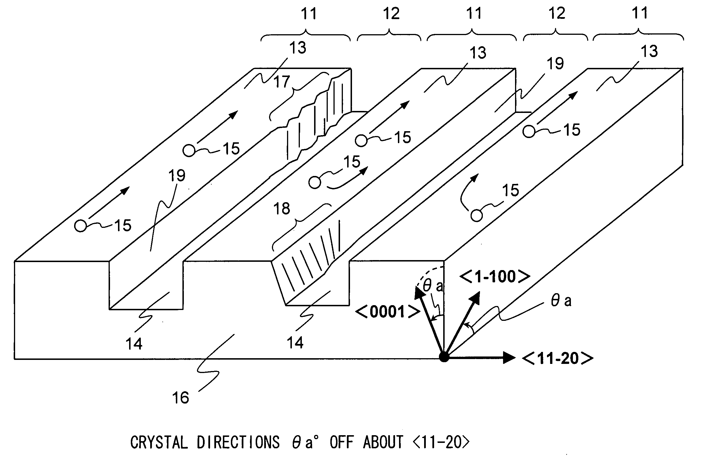
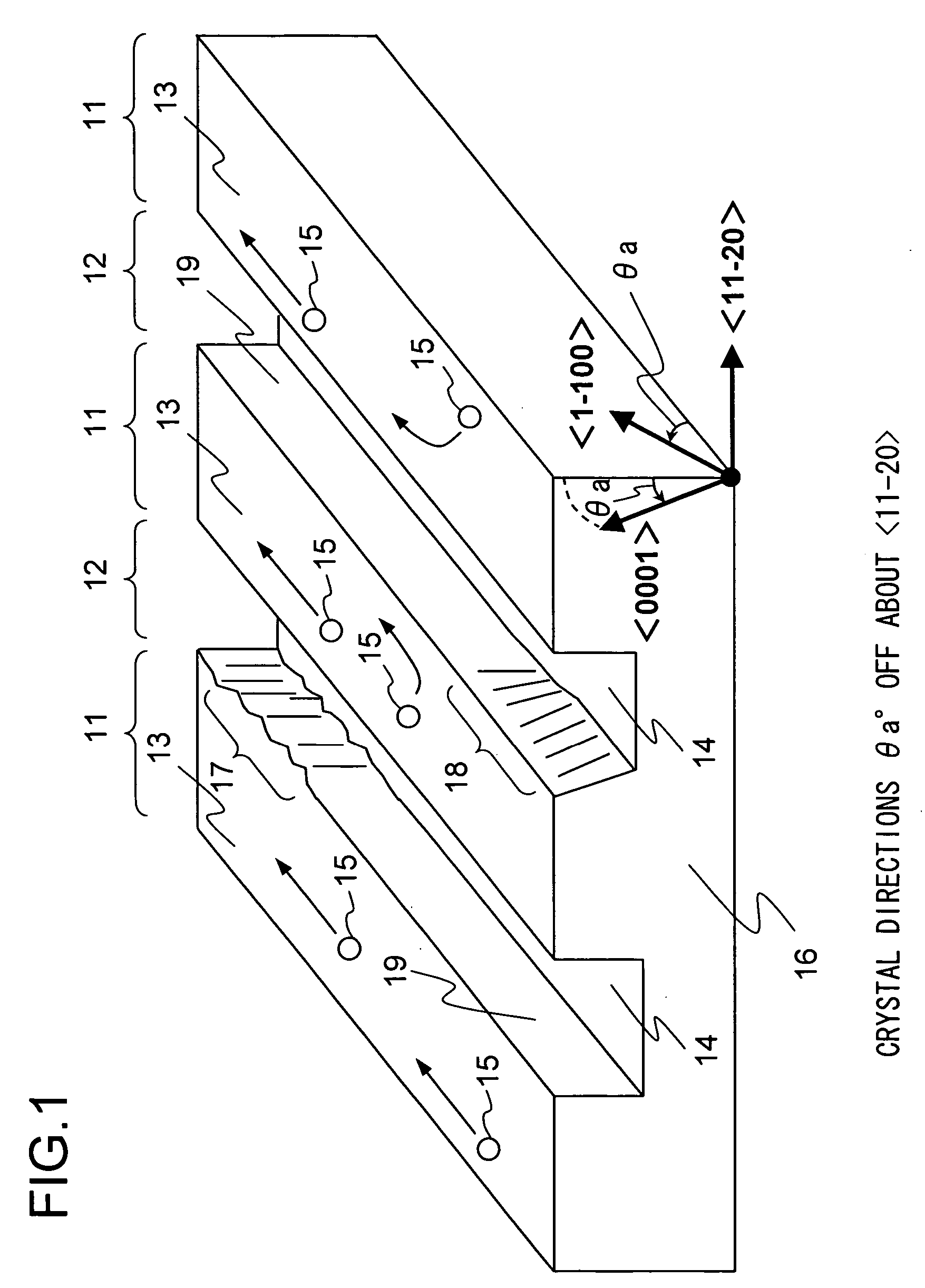
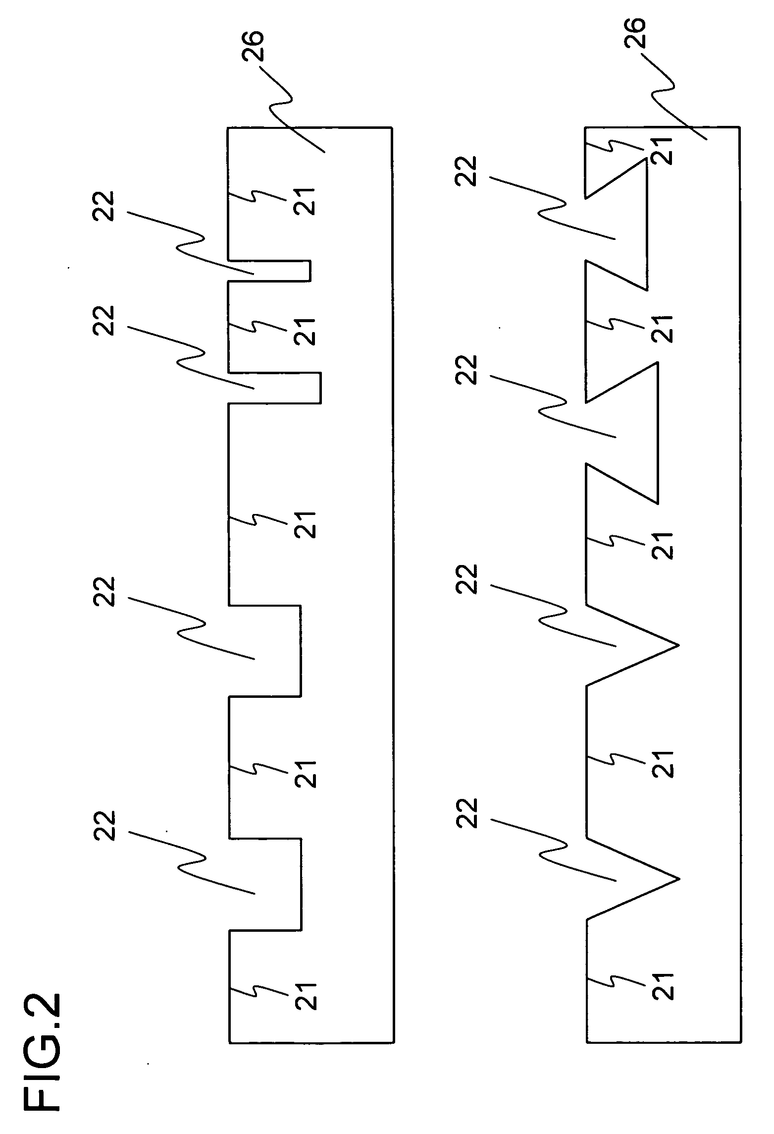
[0088] A first embodiment of the present invention will be described below with reference to the relevant drawings. The following description of embodiments deals with a nitride semiconductor layer as an example of a nitride semiconductor device, but it should be understood that the present invention can be applied to any other type of nitride semiconductor device. FIGS. 1 and 3 are diagrams schematically showing the processed substrates 16 and 36 used in this embodiment, as observed when a nitride semiconductor multiple-layer film 4 is grown thereon. As shown in FIGS. 1 and 3, the processed substrates 16 and 36 each have a fixed off-angle. FIG. 4 is a diagram schematically showing a processed substrate 46 produced from a commonly used substrate having an off-angle of 0.02° or less. In FIGS. 1, 3, and 4, the plane directions are indicated together. In this embodiment, a nitride semiconductor laser device is fabricated by growing a nitride semiconductor multiple-layer film 4 on a pro...

example 1

[0114] Next, a practical example of the first embodiment will be described with reference to the relevant drawings. It should be understood that, although the example presented below deals with, as an example of a nitride semiconductor device, a nitride semiconductor laser device, the present invention is applicable to any other type of nitride semiconductor device. FIG. 11A is a sectional view schematically showing the nitride semiconductor laser device of this example, and FIG. 11B is a top view of FIG. 11A. FIG. 9B is a sectional view schematically showing the processed substrate 90 before the nitride semiconductor thin films are grown thereon in an example of the first embodiment, and FIG. 9A is a top view of FIG. 9B. In FIGS. 9 and 11, the plane directions are indicated together, and it is assumed that the off-angle equals zero. On the processed substrate 90 shown in FIG. 9, a nitride semiconductor multiple-layer film 4 structured, for example, as shown in FIG. 20 is laid to fa...

example 2

[0128] In this example, the processed substrate is produced in the same manner as in Example 1. The differences are: the substrate used to produce the processed substrate has an off-angle θa of −0.05° and an off-angle θb of −0.39°; the opening width of trenches is 80 μm; and the period between adjacent trenches is 300 μm. In other respects, nitride semiconductor laser devices were fabricated in the same manner as in Example 1.

[0129] In this example, as in Example 1, after the nitride semiconductor multiple-layer film 4 is laid on the processed substrate, the surface flatness of the surface of the nitride semiconductor multiple-layer film 4 formed on the ridges was measured. Within the 600 μm wide region so measured, the level difference between the highest and lowest parts of the surface was 24 nm, and thus good surface flatness was obtained.

[0130] Moreover, from among a plurality of nitride semiconductor laser devices of this example fabricated, 100 nitride semiconductor laser de...


PUM


Abstract

A nitride semiconductor device is provided that prevents development of cracks, that has nitride semiconductor thin films with uniform thicknesses and good growth surface flatness, and is thus consistent in characteristics, and that can be fabricated at a satisfactory yield. In this nitride semiconductor device, the nitride semiconductor thin films are grown on a substrate having an off-angle between a direction normal to the surface of ridges and the crystal direction <0001>. This helps either reduce or intentionally promote diffusion or movement of the atoms or molecules of a source material of the nitride semiconductor thin films through migration thereof. As a result, a nitride semiconductor growth layer with good surface flatness can be formed, and thus a nitride semiconductor device with satisfactory characteristics can be obtained.

Description

[0001] This nonprovisional application claims priority under 35 U.S.C. § 119(a) on Patent Application No. 2004-319183 filed in Japan on Nov. 2, 2004 and Patent Application No. 2004-322339 filed in Japan on Nov. 5, 2004, the entire contents of which are hereby incorporated by reference. BACKGROUND OF THE INVENTION [0002] 1. Field of the Invention [0003] The present invention relates to a nitride semiconductor device. More particularly, the present invention relates to a nitride semiconductor device that uses a nitride semiconductor substrate of which at least the surface is formed of a nitride semiconductor, and to a fabrication method of such a nitride semiconductor device. [0004] 2. Description of Related Art [0005] Nitride semiconductors such as GaN, AlGaN, GaInN, and AlGaInN are characterized by having larger band gaps Eg than AlGaInAs- or AlGaInP-based semiconductors and by being direct-transition semiconductor materials. For these reasons, nitride semiconductors have been recei...

Claims


Application Information

Patent Timeline
IPC IPC(8): H01L21/311
CPCH01L21/0237H01L21/0243H01L21/02433H01L21/0254H01L21/02573H01L21/0262H01L29/045H01L29/2003H01L33/16H01L33/32H01S5/32341H01L29/0657
Inventor YAMADA, EIJIKAMIKAWA, TAKESHIARAKI, MASAHIRO
Owner SHARP FUKUYAMA LASER CO LTD
Why Eureka
Try Eureka