[0011] One embodiment of the yield
management system and method in accordance with the present invention provides many advantages over conventional yield management systems and techniques, which make the yield
management system and method in accordance with the present invention more useful to semiconductor manufacturers. The system may be
fully automated and is easy to use, so that no extra training is necessary to make use of the yield management system. In addition, the yield management system handles both continuous and categorical variables. The system also automatically handles
missing data during a processing step that is optimized to consider data for all significant yield parameters. The system can rapidly search through hundreds of yield parameters and generate an output indicating the one or more key yield factors / parameters. The system generates an output preferably in the form of a
decision tree that is easy to interpret and understand. The system may employ advanced splitting rules to parse the data and is also very flexible in that it permits prior yield parameter knowledge from one or more users to be easily incorporated into the building of the model. Unlike conventional yield management systems, if there is more than one
yield factor / parameter affecting the yield of the process, the system can identify all of the parameters / factors simultaneously, so that the
multiple factors / parameters are identified during a
single pass through the yield data.
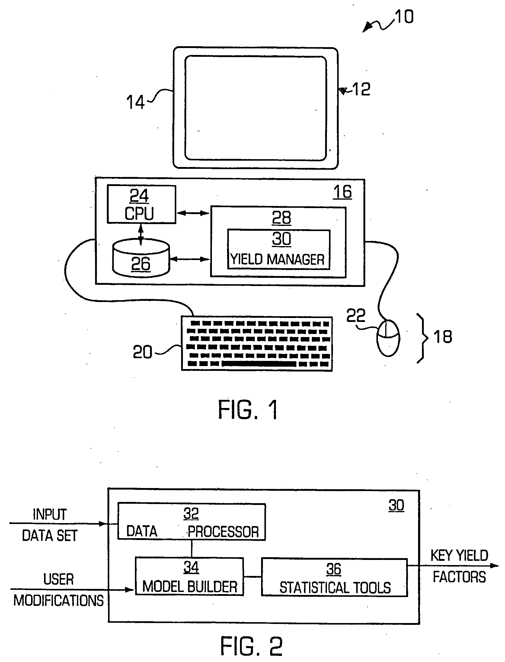
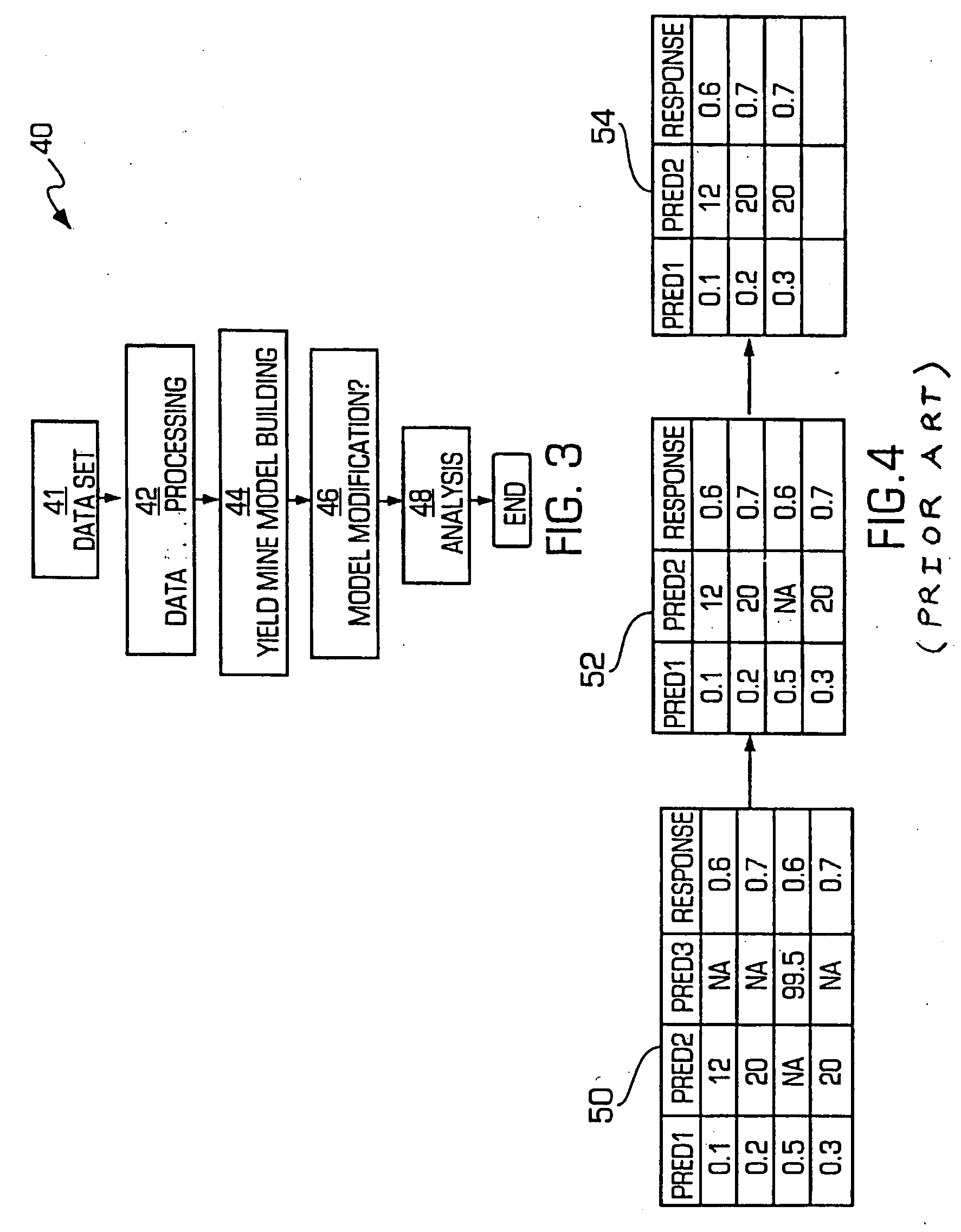
[0012] In accordance with various embodiments of the present invention, the yield management system and method may receive a yield data set. When an input data set is received, one embodiment of the yield management system and method in accordance with the present invention first performs a
data processing step in which the validity of the data in the data set is checked, and cases or parameters with
missing data are identified. One embodiment of the semiconductor yield management system and method in accordance with the present invention provides a tiered splitting method to maximize usage of all valid data points. Another embodiment of the yield management system and method in accordance with the present invention provides an
outlier filtering method. Also, in accordance with various other embodiments of the yield management system and method of the present invention, a user can select from among 1) add tool usage parameters, 2) treat an integer as categorical, and 3) auto-categorize methods for better data manipulation capability and flexibility.
[0013] The semiconductor yield management system and method in accordance with one embodiment of the present invention also preferably provide a linear type split and a range type split for use in constructing the model when the response variable and the prediction variable have a
linear relationship, in order to overcome the shortcoming of a binary
decision tree that has to split on the prediction variable several times on different levels and does not necessarily show that the relationship is linear. The semiconductor yield management system and method in accordance with various embodiments of the present invention also provide
user control in formulating the rules for splitting nodes, so that the user may assure that more appropriate and accurate models are generated. Preferably, the user selectable split methods include: 1) consider tool and date parameters jointly; 2) consider tool and event parameters jointly; 3) maximize class distinction; 4) prefer simple splits; 5) minimum purity; 6) parameter weighting; 7) minimum group size; 8) maximum number of descendants; and 9)
raw data mapping.
[0014] Additionally, if the prediction variable is categorical, one embodiment of the yield management system and method in accordance with the present invention enables the user to select any combination of classes of the variable and include them in one sub-node of the decision tree. The remainder of the data is included in the other sub-node. On the other hand, if the prediction variable is continuous, there are preferably three types of split formats from which the user may select. The available split formats are 1) a default type (a≦X), 2) a range type (a1≦X<a2), and 3) a linear type (X<a1, X in [a1, a2], X in [a2, a3], X>a3). These different split formats facilitate the user being able to produce an accurate model.
[0017] Another embodiment of the yield management system and method in accordance with the present invention additionally enables the user to invoke a method to redisplay the setup window and quickly modify his or her previous selections, so that the model may be adjusted. Finally, the yield management system and method in accordance with another embodiment of the present invention enable the user to invoke methods to collapse / expand a node to collapse the node when the user decides that the split of the node is unnecessary or, alternatively, to expand the node when the user wants to examine the aggregate statistics of the entire subset. The method to expand a node may also be invoked by the user to expand a previously collapsed node, so that the node returns to its original length.
[0018] After the model has been modified, the data set may be processed using various
statistical analysis tools to help the user better understand the relationship between the prediction and response variables. The yield management system and method in accordance with the present invention provide a yield
management tool that is much more powerful and flexible than conventional tools.

