

Components for substrate processing apparatus and manufacturing method thereof
a substrate processing and manufacturing method technology, applied in the direction of liquid surface applicators, electric discharge tubes, coatings, etc., can solve the problems of reducing and affecting the production efficiency of the substrate processing apparatus. , to achieve the effect of preventing a decrease in the operating rate of the substrate processing apparatus, preventing the generation of particle size, and easy manufacturing
- Summary
- Abstract
- Description
- Claims
- Application Information
AI Technical Summary
Benefits of technology
Problems solved by technology
Method used
Image

Examples
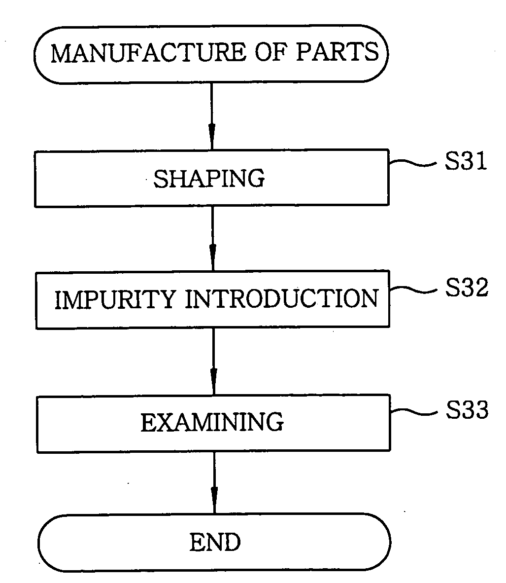
first embodiment
[0029] First, a part for a substrate processing apparatus and a manufacturing method thereof in accordance with the present invention will now be explained.
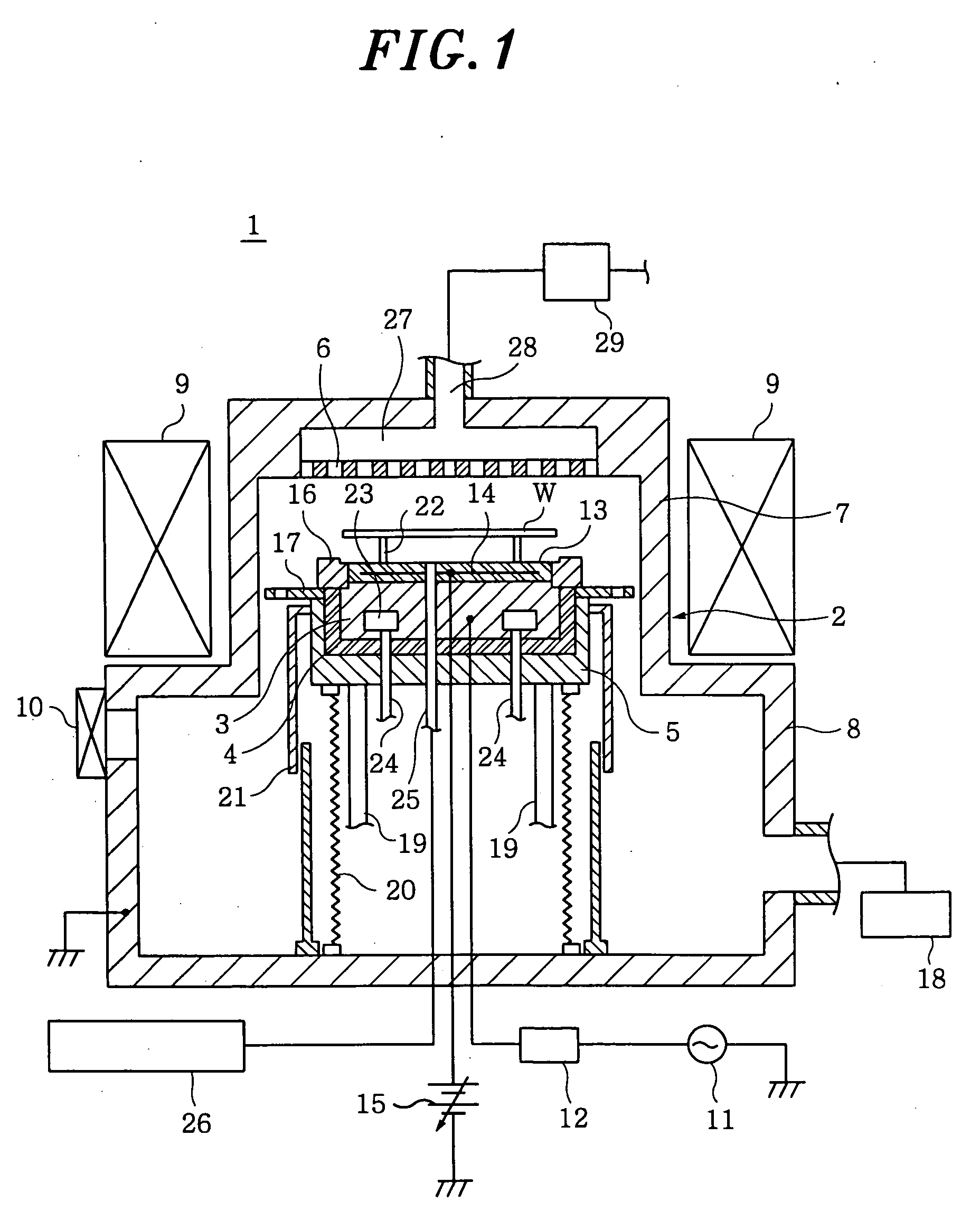
[0030]FIG. 1 is a cross sectional view showing a schematic configuration of a substrate processing apparatus using a focus ring as a part for the apparatus in accordance with a first embodiment of the present invention.
[0031] In FIG. 1, an etching processing apparatus 1 employed as a substrate processing apparatus includes a cylindrical chamber 2 made of, e.g., aluminum; a lower electrode 3, disposed in the chamber 2, for mounting thereon a semiconductor wafer W of, e.g., a 200 mm diameter; an elevatable supporter 5 for supporting the lower electrode 3 through an insulating member 4; and a shower head 6 as an upper electrode, disposed at an upper part of the chamber 2 to face the lower electrode 3.
[0032] The chamber 2 has an upper chamber 7 of a smaller diameter, and a lower chamber 9 of a larger diameter. Around the upper cham...
second embodiment
[0083] In the following, parts for a substrate processing apparatus and a manufacturing method thereof in accordance with the present invention will be explained.
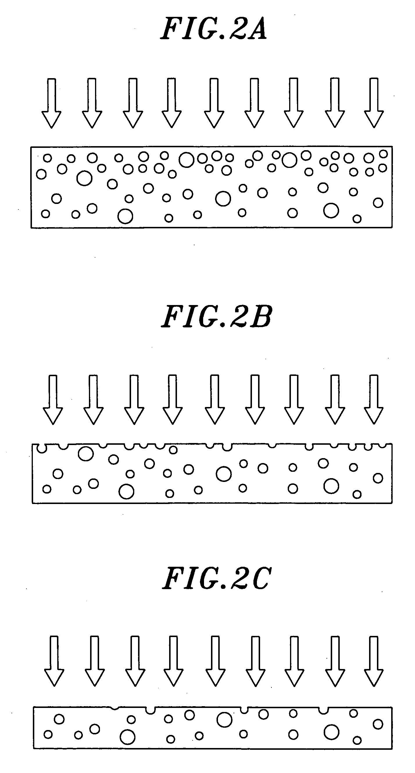
[0084] The present embodiment basically has the same configuration and operation as those of the aforementioned first embodiment, excepting that a heat treatment is employed in lieu of the impurity introduction in the method for manufacturing the parts for the substrate processing apparatus. Therefore, redundant explanations of the same configuration and operation will be omitted, and only the different configuration and operation will be discussed hereinafter.
[0085] In a focus ring employed as a part for a substrate processing apparatus in accordance with the present embodiment, a defect density in the vicinity of a surface thereof is also set to be lower than that in the vicinity of the surface on a CVD silicon carbide body, as in the aforementioned focus ring 16. The focus ring in accordance with the present embodiment ...
PUM
| Property | Measurement | Unit |
|---|---|---|
| temperature | aaaaa | aaaaa |
| diameter | aaaaa | aaaaa |
| depth | aaaaa | aaaaa |
Abstract
Description
Claims
Application Information