

Semiconductor diode and method for the production thereof
a technology of diodes and semiconductors, applied in the field of semiconductor systems, can solve the problems of unfavorable effect, unfavorable effect, and relatively high electrical resistance of semiconductor systems, and achieve the effects of less reverse current, improved resistance, and improved resistan
- Summary
- Abstract
- Description
- Claims
- Application Information
AI Technical Summary
Benefits of technology
Problems solved by technology
Method used
Image

Examples
Embodiment Construction
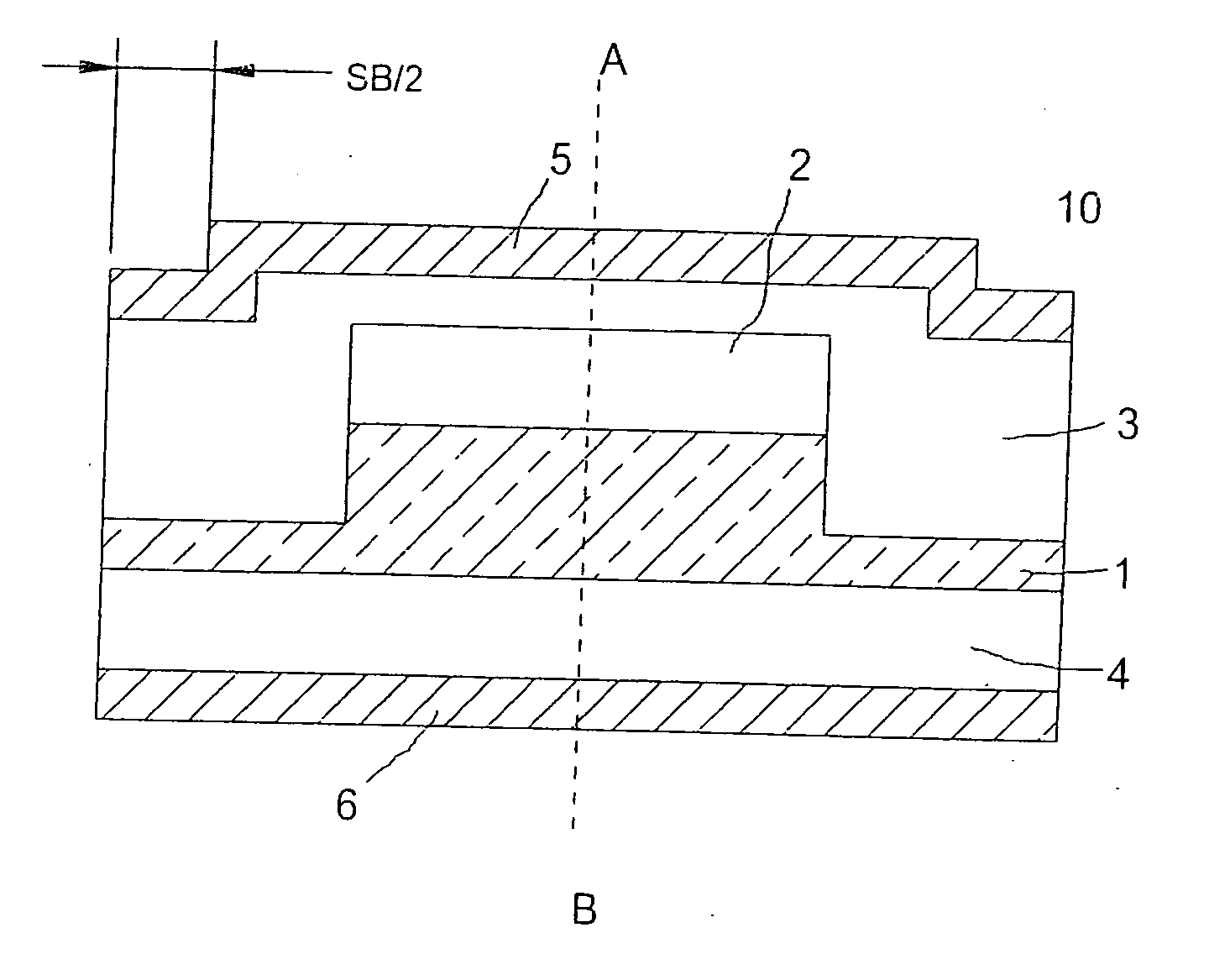
[0013]FIG. 1 first shows a known semiconductor system 10 made up of several variably doped layers 1, 2, 3, 4. Layers 1, 2, 4 are n-doped at different concentrations, while layer 3 is a p-doped layer. The outer surfaces of layers 3 and 4 are coated with contact layers 5, 6 made of metal. This semiconductor system 10 is a diode for example. Together with the n-doped layers 1, 2, p-doped layer 3 forms a p-n junction. Since higher n-doped layer 2 is essentially found only at the center of the semiconductor system, the doping profile at the edges of the diode differs from the doping profile in the central region of the diode. Hence, in reverse-biased operation of the diode, a voltage breakdown at a breakdown voltage UZ essentially only occurs in the central region of the diode and not in its edge region. To be sure, this results in a high robustness in operation since no avalanche breakdown can occur in the edge region of the diode. It is particularly disadvantageous for applications of ...
PUM
 Abstract
Description
Claims
Application Information