Transistor array substrate and display panel

a technology of transistor array and substrate, applied in the direction of electroluminescent light sources, instruments, semiconductor/solid-state device details, etc., can solve the problems of etching accuracy degrade, delay in current flow through interconnection, large change in transistor characteristic,

Active Publication Date: 2006-05-11
SOLAS OLED LTD
View PDF5 Cites 34 Cited by
  • Summary
  • Abstract
  • Description
  • Claims
  • Application Information

AI Technical Summary

Benefits of technology

[0009] It is an object of the present invention to satisfactorily drive a light-emitting element while suppressing any voltage drop and signal delay.
[0035] According to this aspect, the signal lines are patterned together with the gates of the driving transistors. However, since the feed interconnections are stacked on the supply lines, the feed interconnections are formed separately for the drains, sources, and gates of the driving transistors. For this reason, the feed interconnection can be made thick without increasing its width, and the resistance of the feed interconnection can be reduced. Hence, even when a signal is output to the driving transistor and pixel electrode through the feed interconnection, the voltage drop and signal delay can be suppressed.
[0037] According to this aspect, since the feed interconnections can be made thick, the resistance of the feed interconnections can be reduced. When the resistance of the feed interconnections decreases, the signal delay and voltage drop can be suppressed.
[0039] A thick interconnection can suppress the voltage drop and can also be used as a partition wall in forming an organic compound-containing solution. Since the liquid repellent conductive layer exhibits liquid repellency, an organic compound layer can satisfactorily be patterned. A liquid repellent conductive layer containing, e.g., a triazine compound can selectively be formed on a metal surface so as to exhibit liquid repellency but cannot be formed on the surface of an insulator or a metal oxide to exhibit liquid repellency. In addition, the liquid repellent conductive layer is formed on the metal surface very thin. Hence, the electrical conductivity on the metal surface is not lost.

Problems solved by technology

If a current is supplied from the interconnection to a plurality of light-emitting elements, a voltage drop occurs, or the current flow through the interconnection delays due to the electrical resistance of the interconnection.
This may lead to a large change in transistor characteristic.
When the source and drain are formed thick, the etching accuracy of the source and drain degrades.
This may also adversely affect the transistor characteristic.

Method used


Image

  • Transistor array substrate and display panel
  • Transistor array substrate and display panel
  • Transistor array substrate and display panel

Examples


first embodiment

[0068] The best mode for carrying out the present invention will be described below with reference to the accompanying drawing. Various kinds of limitations which are technically preferable in carrying out the present invention are added to the embodiments to be described below. However, the spirit and scope of the present invention are not limited to the following embodiments and illustrated examples.

[Overall Arrangement of EL Display Panel]

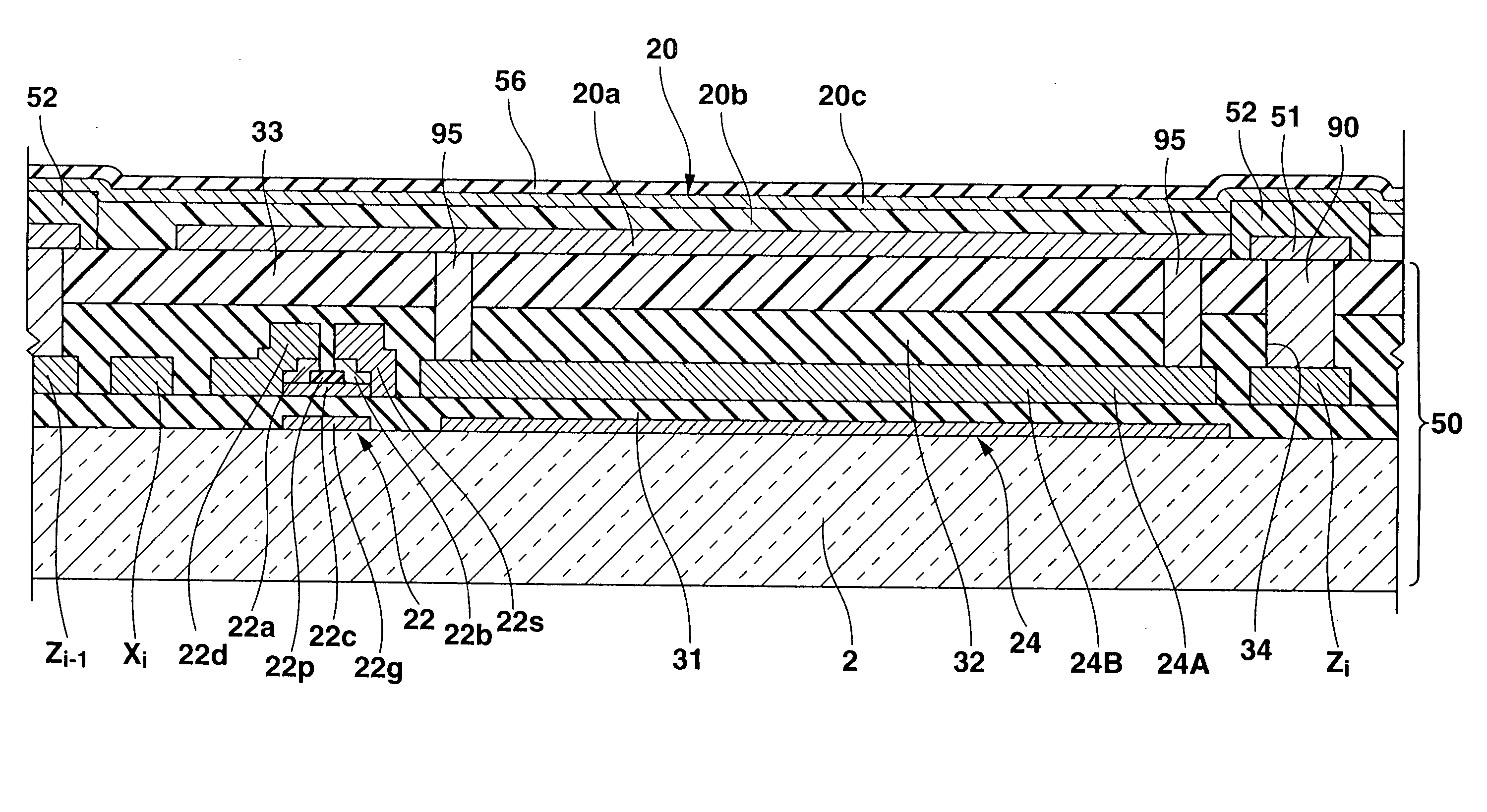
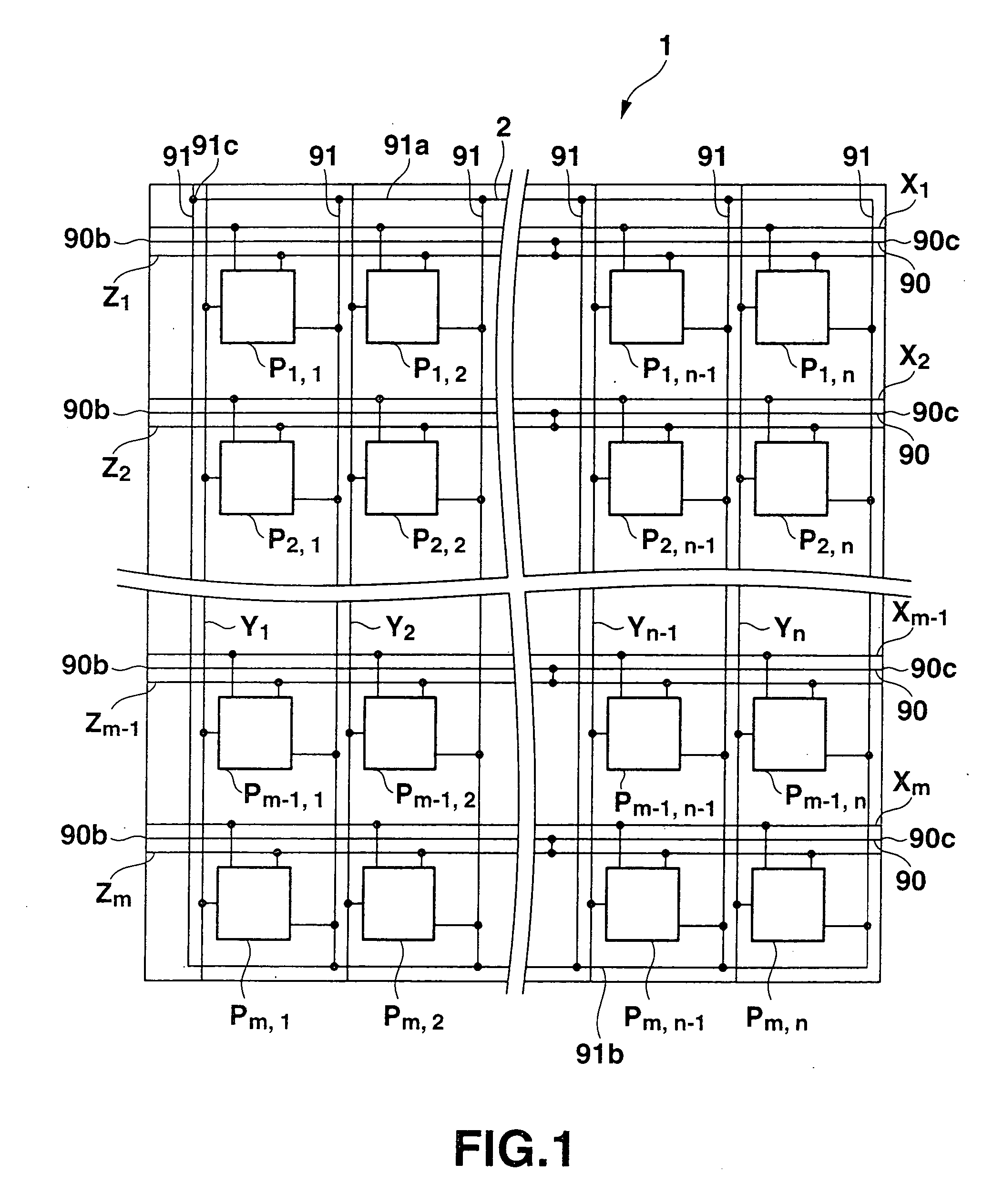
[0069]FIG. 1 is a schematic view showing an EL display panel 1 of active matrix driving type. As shown in FIG. 1, the EL display panel 1 comprises an insulating substrate 2, n (a plurality of) signal lines Y1 to Yn, m (a plurality of) scan lines X1 to Xm, m (a plurality of) supply lines Z1 to Zm, (m×n) pixel circuits P1,1 to Pm,n, a plurality of feed interconnections 90, and common interconnections 91. The insulating substrate 2 is optically transparent and has a flexible sheet shape or a rigid plate shape. The signal lines Y1 to Yn are arraye...

second embodiment

[Overall Arrangement of EL Display Panel]

[0172]FIG. 20 is a schematic view showing an EL display panel 1 of active matrix driving type. As shown in FIG. 20, the EL display panel 1 comprises an insulating substrate 2, n (a plurality of) signal lines Y1 to Yn, m (a plurality of) scan lines X1 to Xm, m (a plurality of) supply lines Z1 to Zm, (m×n) pixel circuits P1,1 to Pm,n, a plurality of feed interconnections 90, and a plurality of common interconnections 91. The insulating substrate 2 is optically transparent and has a flexible sheet shape or a rigid plate shape. The signal lines Y1 to Yn are arrayed on the insulating substrate 2 in parallel to each other. The scan lines X1 to Xm are arrayed on the insulating substrate 2 to be perpendicularly to the signal lines Y1 to Yn when the insulating substrate 2 is viewed from the upper side. The supply lines Z1 to Zm are arrayed on the insulating substrate 2 between the scan lines X1 to Xm to be parallel to them so that the supply lines an...

first modification

[First Modification]

[0219] The present invention is not limited to the above-described embodiments, and various changes and modifications can be made without departing from the spirit and scope of the present invention.

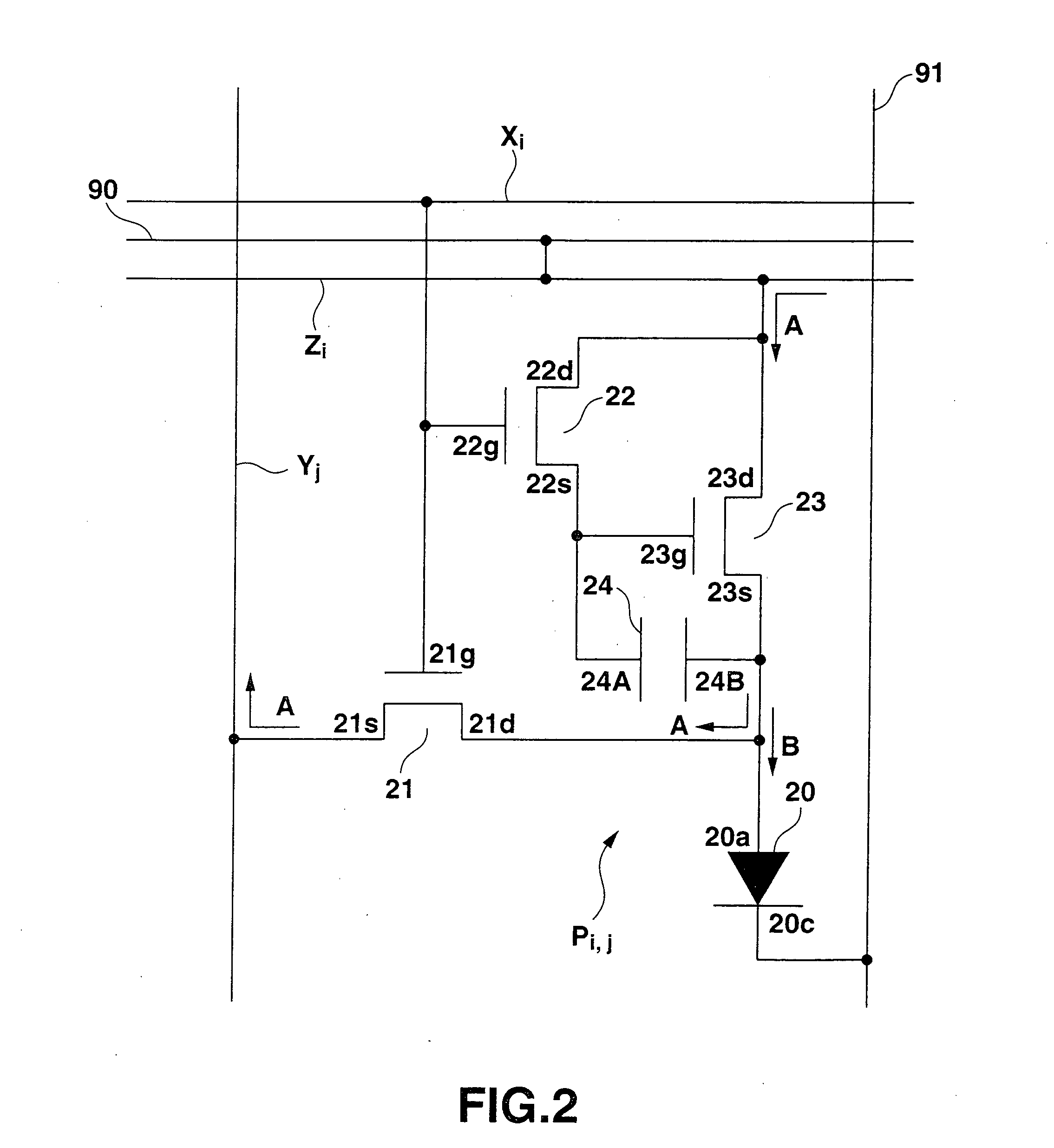
[0220] In the above embodiments, the first to third transistors 21 to 23 have been explained as N-channel field effect transistors. The transistors 21 to 23 may be P-channel field effect transistors. In this case, the relationship between the sources 21s, 22s, and 23s of the transistors 21 to 23 and the drains 21d, 22d, and 23d of the transistors 21 to 23 is reversed in the circuit diagram shown in FIG. 2. For example, when the driving transistor 23 is a P-channel field effect transistor, the drain 23d of the driving transistor 23 is electrically connected to the pixel electrode 20a of the organic EL element 20. The source 23s is electrically connected to the supply line Zi.


PUM


Abstract

A transistor array substrate includes a plurality of driving transistors which are arrayed in a matrix on a substrate. The driving transistor has a gate, a source, a drain, and a gate insulating film inserted between the gate, and the source and drain. A plurality of signal lines are patterned together with the gates of the driving transistors and arrayed to run in a predetermined direction on the substrate. A plurality of supply lines are patterned together with the sources and drains of the driving transistors and arrayed to cross the signal lines via the gate insulating film. The supply line is electrically connected to one of the source and the drain of the driving transistor. A plurality of feed interconnections are formed on the supply lines along the supply lines, respectively.

Description

CROSS-REFERENCE TO RELATED APPLICATIONS [0001] This application is based upon and claims the benefit of priority from prior Japanese Patent Applications No. 2004-273532, filed Sep. 21, 2004; No. 2004-273580, filed Sep. 21, 2004; and No. 2005-269434, filed Sep. 16, 2005, the entire contents of all of which are incorporated herein by reference. BACKGROUND OF THE INVENTION [0002] 1. Field of the Invention [0003] The present invention relates to a transistor array substrate having a plurality of transistors and, more particularly, to a display panel using light-emitting elements which cause self emission when a current is supplied by the transistor array substrate. [0004] 2. Description of the Related Art [0005] Organic electroluminescent display panels can roughly be classified into passive driving types and active matrix driving types. Organic electroluminescent display panels of active matrix driving type are more excellent than those of passive driving type because of high contrast ...

Claims


Application Information

Patent Timeline
Patent Type & Authority Applications(United States)
IPC IPC(8): G11C8/00
CPCH01L27/124H05B33/22H05B33/10
Inventor SHIMODA, SATORUSHIRASAKI, TOMOYUKIOGURA, JUNKUMAGAI, MINORU
Owner SOLAS OLED LTD
Why Eureka
Try Eureka