Phase shift mask fabrication method thereof and fabrication method of semiconductor apparatus

Inactive Publication Date: 2006-05-11
SONY CORP
View PDF10 Cites 25 Cited by
  • Summary
  • Abstract
  • Description
  • Claims
  • Application Information

AI Technical Summary

Benefits of technology

[0012] According to the present invention, there is provided an exposure light phase shift mask devised to attain the above object, that is, an exposure light phase shift mask used to transfer a desired pattern to a light exposed material by a reflection of an exposure light, the phase shift mask being characterized by having a reflective mask blank with multilayered films that reflects the exposure light, and a first and

Problems solved by technology

On the contrary, as for the extreme ultraviolet radiation having the wavelength of 13.5 nm, there is no material that allows the above extreme ultraviolet radiation to be transmitted through a desired thickness.
However, while the transparent mask that is of a light transmitting type is easy to constitute the phase shift mask as is generally known, the reflective mask adapted to the extreme ultraviolet radiation has a quite difficulty in configuring the phase shift mask.
For instance, the transparent mask allows regions different in optical phase difference by 180° to be formed using a means of digging in a mask blank, in which case, however, an application of the above means to the reflective mask as it is causes also a change of an optical reflectance simultaneously with a digging-in of the m

Method used


Image

  • Phase shift mask fabrication method thereof and fabrication method of semiconductor apparatus
  • Phase shift mask fabrication method thereof and fabrication method of semiconductor apparatus
  • Phase shift mask fabrication method thereof and fabrication method of semiconductor apparatus

Examples


first embodiment

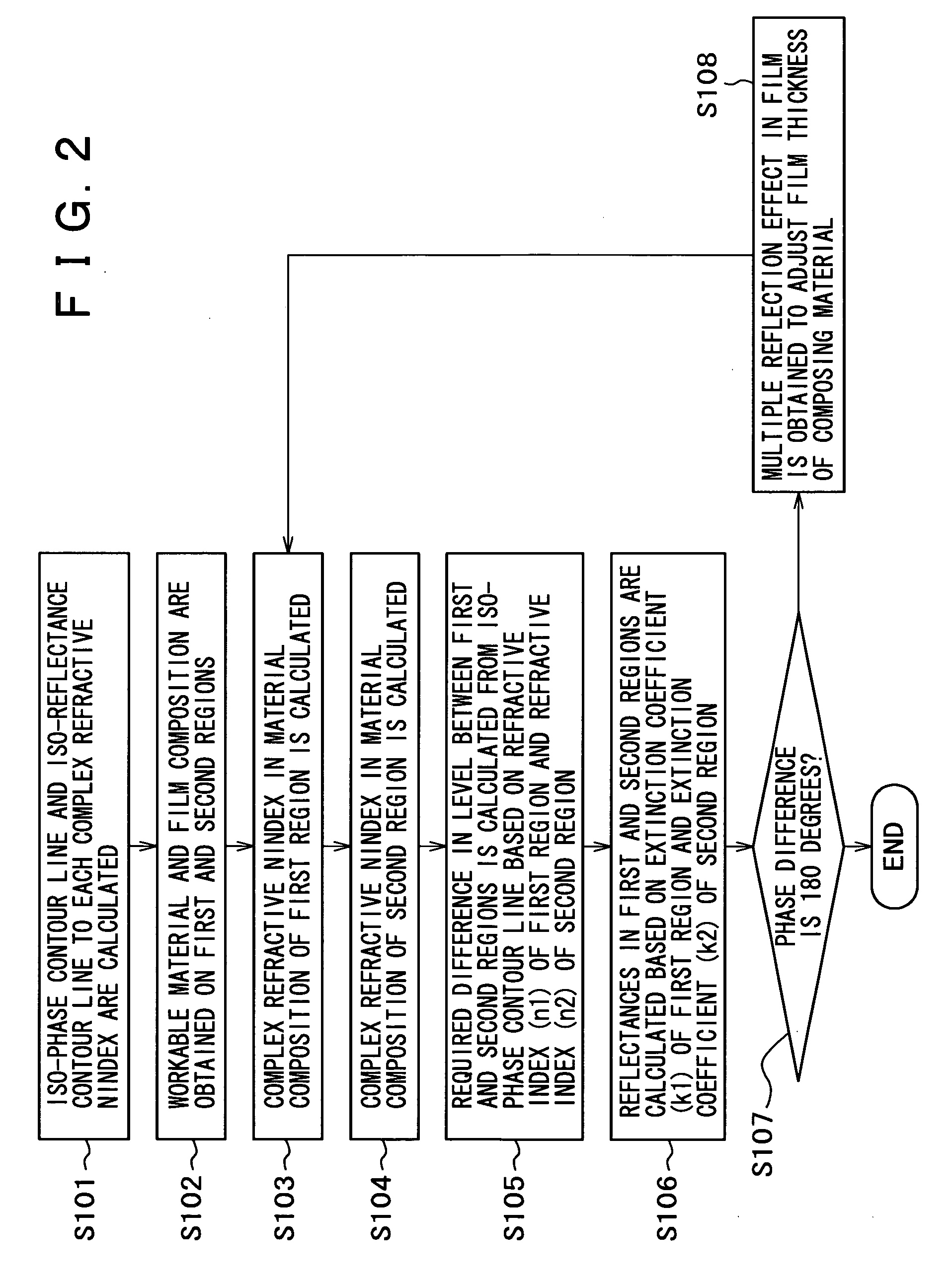
[0080] The first embodiment is described by taking the case where the present invention is applied to constitute a halftone phase shift mask. FIG. 2 is a flow chart showing the fabrication procedure of the phase shift mask in the first embodiment.

[0081] In a fabrication of the halftone phase shift mask, an iso-phase contour line and an iso-reflectance contour line to each complex refractive index are firstly calculated (Step 101, where Step is hereinafter abbreviated to “S”). A calculation of the iso-phase contour line and the iso-reflectance contour line is required for an arbitrary complex refractive index without being limited to the existing material. That is, with reference to the arbitrary complex refractive index to the extreme ultraviolet radiation, a phase and a reflectance of the reflected light contained in the extreme ultraviolet radiation based on the above arbitrary complex refractive index are specified. Incidentally, the phase and the reflectance to the complex refr...

second embodiment

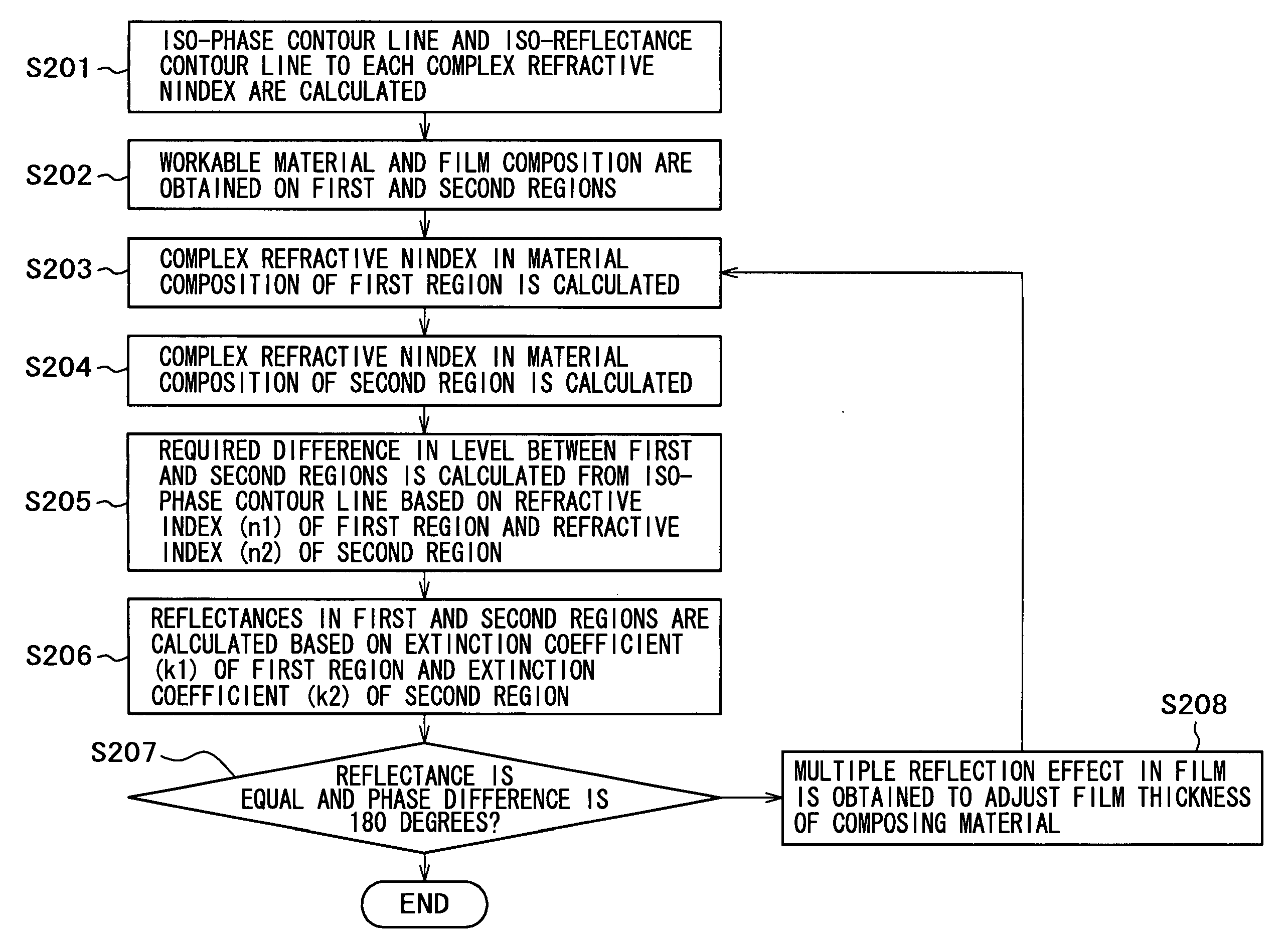
[0097] The second embodiment of the fabrication procedure of the phase shift mask is now described. A description of the second embodiment is given by taking the case where the present invention is applied to constitute a Levenson phase shift mask. FIG. 14 is a flowchart showing the fabrication procedure of the phase shift mask in the second embodiment.

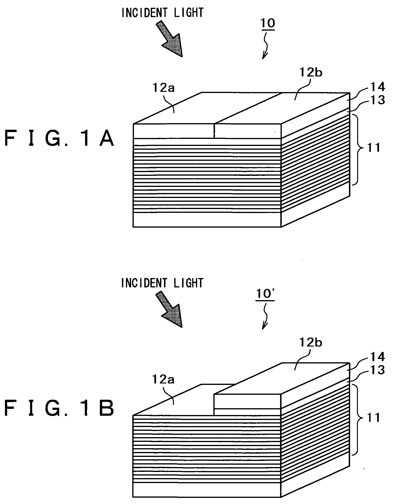
[0098] As shown in FIG. 14, the fabrication of the Levenson phase shift mask is also performed approximately in the same manner (See FIG. 2) as that in the case of the halftone phase shift mask in the above first embodiment (S201 to S208). However, the Levenson phase shift mask is different from the halftone phase shift mask in that the former requires that not only the phases in the first region 12a and the second region 12b are different by 180°, but also the reflectance in the first region 12a and that in the second region 12b are approximately equal. That is, for constituting the Levenson phase shift mask, it is necessary to sati...


PUM


Abstract

There is disclosed an extreme ultraviolet phase shift mask that may be constituted practically by obtaining an appropriate combination of a refractive index with an absorption coefficient, even in the case of a reflection of an extreme ultraviolet radiation. When constituting a phase shift mask (10) having a reflective mask blank with multilayered films (11) that reflects a short ultraviolet light and a first and a second regions (12a) and (12b) formed on the reflective mask blank with multilayered films (11), firstly, with reference to an arbitrary complex refractive index to the extreme ultraviolet radiation and an arbitrary thickness of a film, a phase and a reflectance of a reflected light contained in the extreme ultraviolet radiation based on the above complex refractive index and the above film thickness are specified. Then, each film thickness and each complex refractive index in formative films of the first and the second regions (12a) and (12b) are set based on the specific results of the phase and the reflectance to ensure that the reflected light contained in the exposure light in the first region (12a) and the reflected light contained in the exposure light in the second region (12b) create a prescribed phase difference.

Description

TECHNICAL FIELD [0001] The present invention relates to a phase shift mask for use in a lithography process for forming a circuit pattern of a semiconductor apparatus, a fabrication method thereof, and a fabrication method of a semiconductor apparatus including the lithography process, and more particularly, to a phase shift mask adaptable to so-called extreme ultraviolet radiation, a fabrication method thereof, and a fabrication method of a semiconductor apparatus. BACKGROUND ART [0002] In recent years, with a micro-miniaturization of a semiconductor apparatus, a minimization of a pattern width (a line width) and an inter-pattern pitch, etc. have been required for a circuit pattern formed on a wafer and a resist pattern, etc. for forming the circuit pattern. Such requirement for the above minimization is satisfied by further shortening a wavelength of an ultraviolet light for use in an exposure of a resist. As the micro-miniaturization of the semiconductor apparatus has advanced, t...

Claims


Application Information

Patent Timeline
IPC IPC(8): G03C5/00G06F17/50G03F1/00
CPCB82Y10/00B82Y40/00G03F1/30G03F1/26G03F1/24
Inventor SUGAWARA, MINORU
Owner SONY CORP
Why Eureka
Try Eureka