

Method for improving optical proximity correction
- Summary
- Abstract
- Description
- Claims
- Application Information
AI Technical Summary
Benefits of technology
Problems solved by technology
Method used
Image

Examples
Embodiment Construction
[0037] In the following description, numerous specific details may be set forth to provide a thorough understanding of the present invention. However, it will be obvious to those skilled in the art that the present invention may be practiced without such specific details.
[0038] Refer now to the drawings wherein depicted elements are not necessarily shown to scale and wherein like or similar elements are designated by the same reference numeral through the several views.
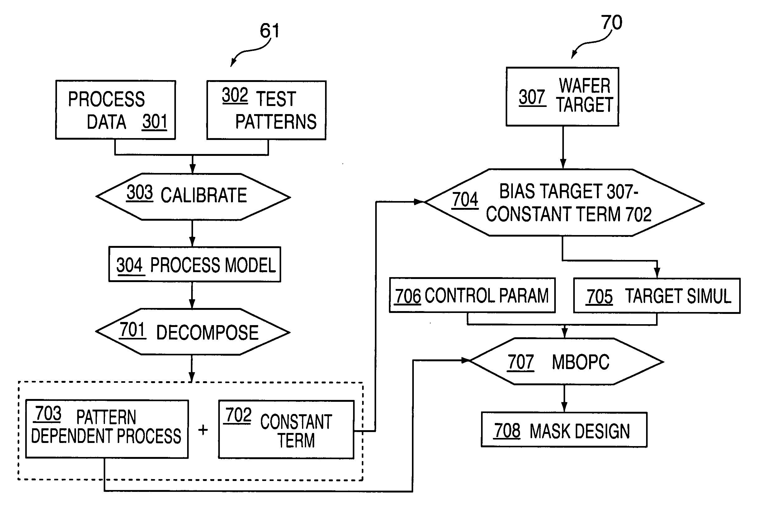
[0039] Referring to FIG. 3, a flow diagram of a conventional model based optical proximity correction (MBOPC) process is illustrated. The MBOPC process consists of two major sections: the creation of a model, referred to as Model Build 60, including Blocks 301-304, and the use of that model to create a photomask design based on the design of the semiconductor integrated circuit to be formed on a wafer, referred to as Data Prep 30, including Blocks 307-310. The model build process 60 is generally carried out one time...
PUM
 Abstract
Description
Claims
Application Information