Wafer fab

a technology of wafer fab and fab sheet, which is applied in the direction of coating, chemical vapor deposition coating, metallic material coating process, etc., can solve the problems of increasing the need for expensive and special facilities, increasing the cost of manufacturing in the wafer fab area, and reducing the space required. , the effect of preventing breakag

Inactive Publication Date: 2006-05-18
INTEVAC
View PDF18 Cites 142 Cited by
  • Summary
  • Abstract
  • Description
  • Claims
  • Application Information

AI Technical Summary

Benefits of technology

[0004] The invention described addresses these problems. It reduces space required for the wafer transport subsystem so that it does not occupy physical floor space or a footprint beyond that occupied by the processing subsystems. In essence wafer handling mechanism is within the space generally occupied by the processing stations. The system includes multiple chambers and wafers are transported from chamber to chamber in a series and parallel sense as will be described in more detail hereinafter. At an early point, such as at the point of entry of the wafer into the load lock, wafers are combined with a supporting chuck and the wafer travels through the system back to the load lock in position on the chuck. This has an effect of lowering costs and preventing breakage in the processing of thin substrates. Transport of wafers between chambers takes place in series in the sense that a wafer passes from a processing chamber to the next adjacent processing chamber and in parallel in that all wafers in a row of chambers are moved at the same time by moving all wafers at once from chamber to chamber, and transfer of wafer between chambers does not otherwise occur. In addition the time of treatment within chambers is the same for each chamber. Additionally, the equipment may be structured for the same process or for more than a single process or for an insulating chamber to completely separate operating processes. It is also possible to obtain the benefits of sharing aux

Problems solved by technology

Recycling involves delays and expenses since once the processing chamber is opened and exposed to atmospheric conditions, a pump down would be required before a next batch could be cycled or processed through the system.
Because of wafer transfer and other wafer handling considerations in going from equipment to equipment, the need for ultra clean clean-rooms developed and this, plus the large footprint occupied by the multiple machines or tools, operating within the clean room increased further the need for expensive and special facilities and in turn the expense of manufacturing in the wafer fab area.
In addition these units may cost in excess of a few million dollars per unit and needless to say there are other manufacturers of semiconductor manufacturing equipment offering other units for different processes for processing wafers which are also used in the fab line.
Setting up a new fab line today can cost two or more billion dollars, a significant investment for any business.
As discussed such systems

Method used


Image

  • Wafer fab
  • Wafer fab
  • Wafer fab

Examples


Embodiment Construction

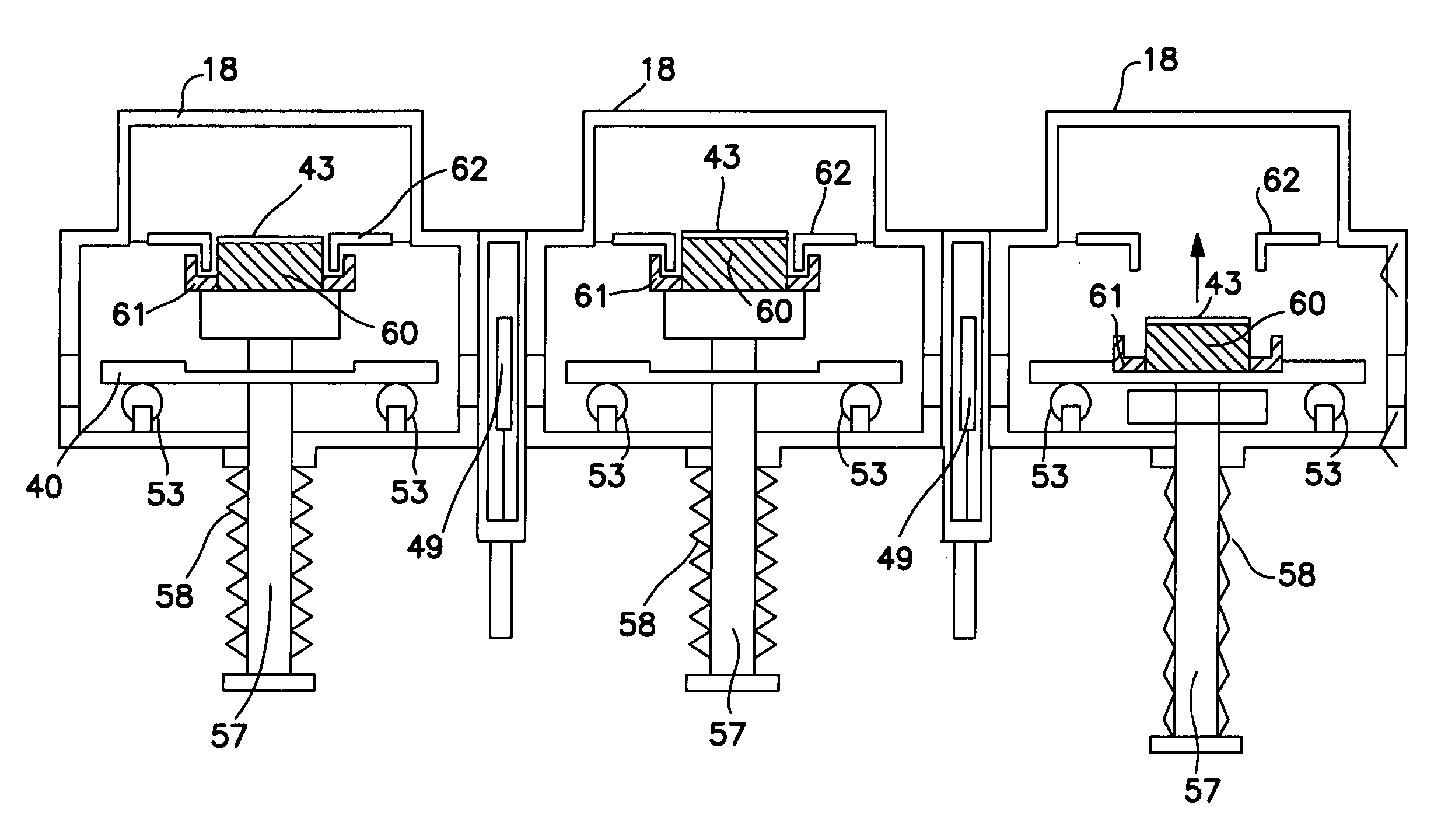
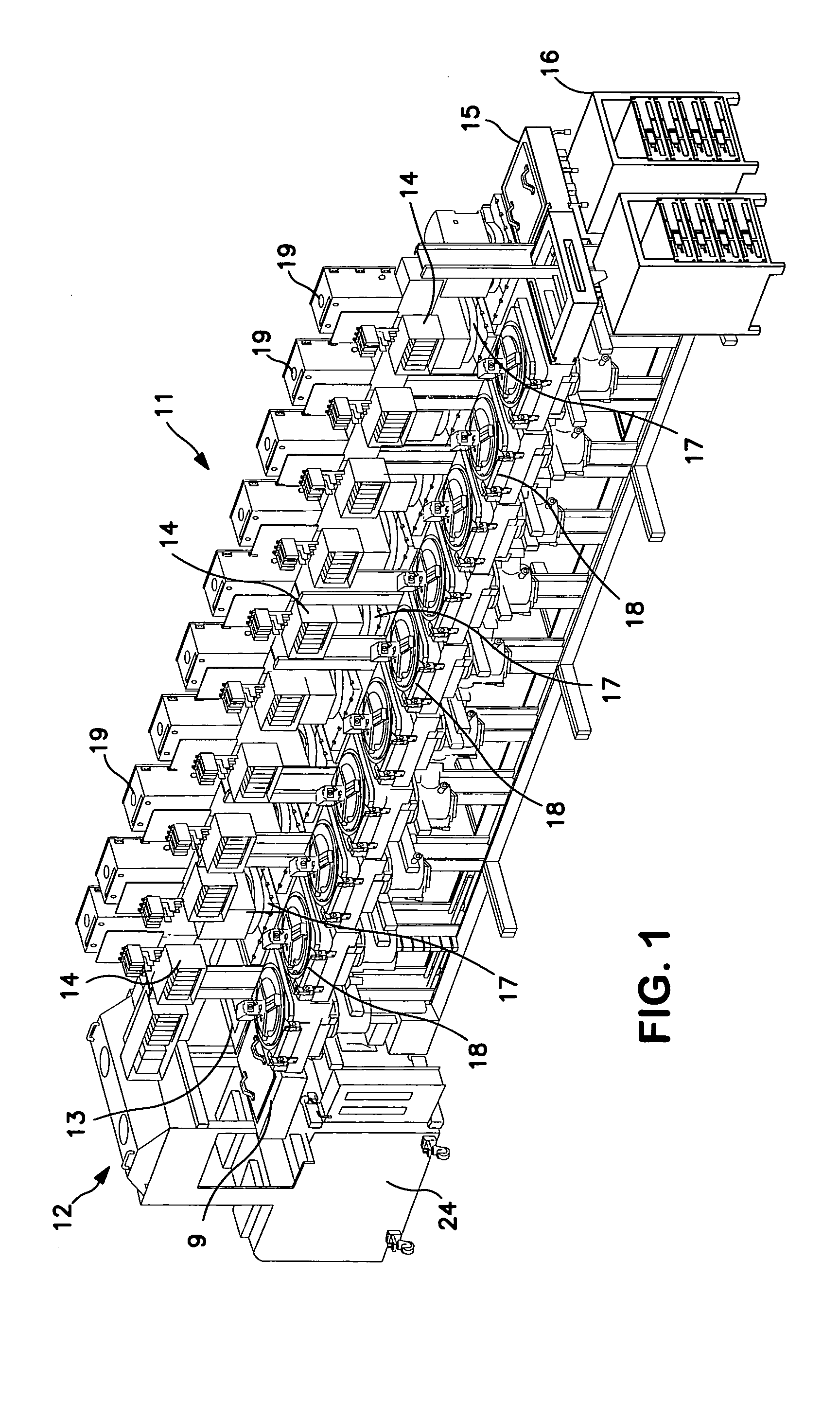
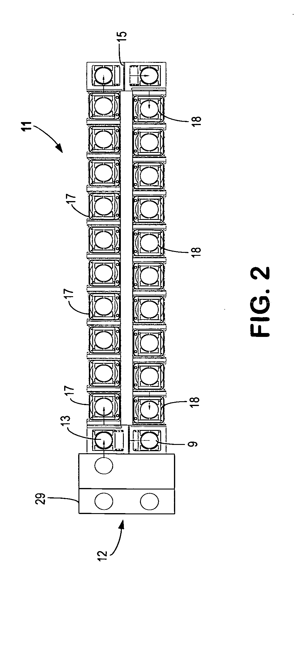
[0016] Referring now to FIG. 1, there is shown as an example of an embodiment of this invention, a 20 station system. Although in this Figure, a certain number of stations are shown, it should be understood that this invention may be practiced in a system with more or less stations depending on the needs at the installation. Also different stations are illustrated on the left side compared to the right side (which in the Figure appears as in the rear or in the front, respectively). However, a selection of stations may be made other than the ones shown and the unit will function in accordance with its intended purpose. In this Figure, 11 represents the 20 station system. The front end of the system 12 is where load lock 13 is located. At the opposite end is a transverse or shuttle chamber 15 and power supplies 16 for the process chambers, transport systems and other mechanisms of the system. In this Figure, like appearing process modules 17, appear along the left side viewing from th...


PUM

PropertyMeasurementUnit
Timeaaaaaaaaaa
Sizeaaaaaaaaaa
Transport propertiesaaaaaaaaaa

Abstract

Described is a method for manufacturing wafers and a manufacturing system in which the footprint is substantially contained in a size approximating the processing chambers. Single wafers move horizontally through the system and processing occurs simultaneously in groups of processing chambers. Various manufacturing processes employed in making semiconductor wafers are included as processing chambers in the system.

Description

FIELD OF THE INVENTION [0001] This invention has to do with wafer fabrication and in particular with a modular system in a universal fab tool for wafer manufacturing. BACKGROUND OF THE INVENTION [0002] Wafers were historically processed in batches. Thus a batch of wafers, in for example, a cassette were exposed to a process step. They were then removed from the equipment and the equipment was recycled for a next batch. Recycling involves delays and expenses since once the processing chamber is opened and exposed to atmospheric conditions, a pump down would be required before a next batch could be cycled or processed through the system. The batch would then be carried through a next process step. After years, the batch system progressed to single wafer processing units. A history of these developments is traced in U.S. Pat. No. 4,756,815, which also describes a sputter coating system operating in a single wafer, rather than the batch, mode. In essence the value produced working on a ...

Claims


Application Information

Patent Timeline
IPC IPC(8): C23C16/00H01L21/306
CPCH01L21/67161H01L21/67173H01L21/6719H01L21/67201H01L21/67745
Inventor FAIRBAIRN, KEVIN P.PONNEKANTI, HARILANE, CHRISTOPHERWEISS, ROBERT EDWARDLATCHFORD, IANBLUCK, TERRY
Owner INTEVAC
Why Eureka
Try Eureka