Method of fabricating flash memory

Inactive Publication Date: 2006-05-18
POWERCHIP SEMICON CORP
View PDF4 Cites 17 Cited by
  • Summary
  • Abstract
  • Description
  • Claims
  • Application Information

AI Technical Summary

Benefits of technology

[0011] The invention provides a method for fabricating a flash memory by forming the floating gate and the control gate in a self-aligned way, thus simplifying the fabrication processes. The method of the present invention can also increase the gate couple ratio between the floating gate and the control gate and improve the yield of the products.

Problems solved by technology

As the microprocessor of the computer becomes more powerful and the programming of the software becomes more complex, the demands for large-capacity memory devices keep increasing.
Due to many uncontrollable factors of photolithography, misalignment often occurs to the floating gates during the photolithography process, and the fabricating process is more complicate.
However, as the integration of the device becomes higher and the size of the device is minimized based on the design rule, it is difficult to increase the overlapped area of the control gate and the floating gate, and it therefore has the issues for incapable of increasing the GCR between the floating gate and the control gate, and increasing the device integration.

Method used


Image

  • Method of fabricating flash memory
  • Method of fabricating flash memory
  • Method of fabricating flash memory

Examples


Embodiment Construction

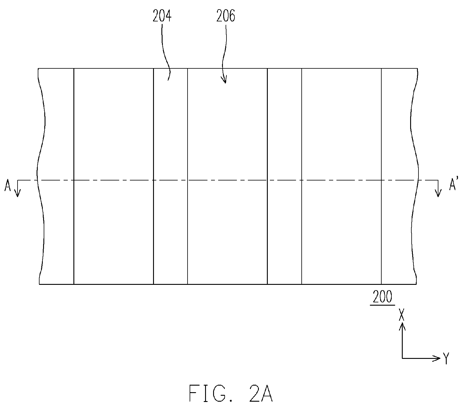
[0032]FIGS. 2A-2E are top views illustrating the process steps for forming a flash memory structure according to one preferred embodiment of the present invention. FIGS. 3A-3E are cross-sectional views illustrating the process steps for forming the flash memory structure of FIGS. 2A-2E along the line A-A′, according to the preferred embodiment of the present invention.

[0033] Referring to FIGS. 2A and 3A, a substrate 200, for example, a silicon substrate is provided. A pad layer 202 is formed on the substrate 200. The material of the pad layer 202 can be silicon oxide formed by thermal oxidation, for example. A mask layer 204 is formed over the substrate 200. The material of the mask layer 204 has an etching selectivity different from that of the subsequently formed floating gate or control gate. The material of the mask layer 204 is silicon nitride formed by chemical vapor deposition (CVD), for example. Later on, the mask layer 204 is patterned to form a plurality of trenches 206 t...


PUM


Abstract

A method of fabricating a flash memory is provided. The method includes forming a mask layer with first openings on the substrate. A tunneling dielectric layer is formed at bottom in the first openings. Strips of conductive spacers are formed on sidewalls of the first openings, and source / drain regions are formed in the substrate within the first openings. The strips of conductive spacers are patterned to form floating gates. A first inter-gate dielectric layer is formed over the substrate. Control gates are formed on the substrate to fill the first openings. Mask layer is removed to form second openings. Gate dielectric layer is formed at bottom of second openings, and second inter-gate dielectric layer is formed on the sidewalls of floating gates, and the sidewalls and top surface of the control gates. Word lines are formed to fill second openings disposed between the floating gates and cover the control gates.

Description

CROSS-REFERENCE TO RELATED APPLICATION [0001] This application claims the priority benefit of Taiwan application serial no. 93134870, filed on Nov. 15, 2004. All disclosure of the Taiwan application is incorporated herein by reference. BACKGROUND OF THE INVENTION [0002] 1. Field of Invention [0003] The present invention relates to a method of fabricating a semiconductor device. More particularly, the present invention relates to a method for fabricating a flash memory. [0004] 2. Description of Related Art [0005] As the microprocessor of the computer becomes more powerful and the programming of the software becomes more complex, the demands for large-capacity memory devices keep increasing. The current trend of memory fabrication process for an integrated circuit is to increase the storage density and the data storage amount in the memory device. In order to fabricate cheap and large-capacity memories, the dimension of the memories keeps shrinking and the integration of the memories ...

Claims


Application Information

Patent Timeline
IPC IPC(8): H01L29/788
CPCH01L27/115H01L27/11521H10B69/00H10B41/30
Inventor CHANG, KO-HSINGCHANG, SU-YUAN
Owner POWERCHIP SEMICON CORP
Why Eureka
Try Eureka