Multi-layer high quality gate dielectric for low-temperature poly-silicon TFTs

a polysilicon and gate dielectric technology, applied in the field of multi-layer high-quality gate dielectric layer and p-si/gate dielectric interface, can solve the problems of inability to meet the highest tft device performance needs, the quality of the interface between the deposited film and the p-si channel layer is often not satisfactory, and the process to form a good interface between the deposited film and the p-si channel layer is often not possible. achieve high quality and

Inactive Publication Date: 2006-05-18
APPLIED MATERIALS INC
View PDF84 Cites 59 Cited by
  • Summary
  • Abstract
  • Description
  • Claims
  • Application Information

AI Technical Summary

Benefits of technology

[0012] The present invention generally provides a method of plasma processing a substrate. The method comprises moving the substrate to a first of a plurality of processing positions in a plasma processing region of a plasma processing chamber, flowing an oxidizing gas mixture into the plasma processing region, generating a plasma in the plasma processing region at a substrate surface temperature of no more than about 550° C. to form an oxidized surface on the substrate, moving the substrate to a second of the plurality of processing positions, and forming a dielectric layer on the surface of the substrate to form a gate dielectric layer having a thickness from about 100 Å to about 6000 Å.
[0013] The present invention generally provides a method of plasma processing a substrate. The method comprises moving the substrate to a first of a plurality of processing positions in a plasma processing region of a plasma processing chamber, flowing an oxidizing gas mixture into the plasma processing region, generating a plasma in the plasma processing region at a substrate surface temperature of no more than about 550° C. using a first RF transmitting device, moving the substrate to a second of a plurality of processing positions in a plasma processing region of a plasma processing chamber, flowing a dielectric layer forming gas mixture into the plasma processing region; and generating a plasma in the plasma processing region at a substrate surface temperature of no more than about 550° C. using a second RF transmitting device to form a dielectric layer on the surface on the substrate.
[0014] The present invention generally provides a cluster tool for forming a high quality gate oxide layer on a substrate. The cluster tool comprises a plurality of plasma processing chambers adapted for forming an oxidized surface on the substrate and depositing a dielectric layer on the substrate to form a gate dielectric l

Problems solved by technology

The quality of the p-Si channel layer film has received a lot of attention in recent years, while the creation of a high quality gate dielectric layer and p-Si/gate dielectric interface has been elusive.
The gate dielectric layer 4 typically comprises an oxide, deposited using conventional techniques, such as, for example, PECVD, which is commonly deposited between about 350° C. and about 450° C. Unfortunately, the quality of the interface between the deposited film and the p-Si channel layer is often not

Method used


Image

  • Multi-layer high quality gate dielectric for low-temperature poly-silicon TFTs
  • Multi-layer high quality gate dielectric for low-temperature poly-silicon TFTs
  • Multi-layer high quality gate dielectric for low-temperature poly-silicon TFTs

Examples


Embodiment Construction

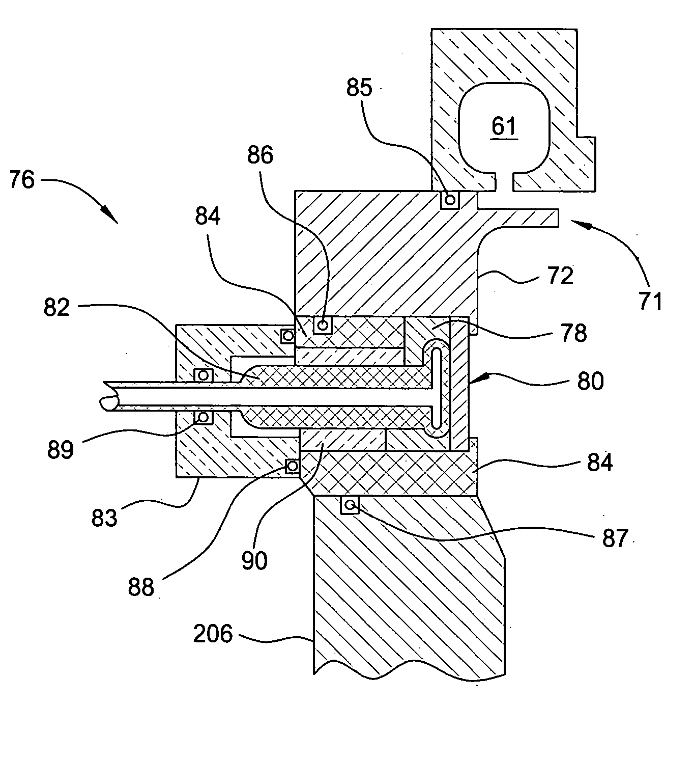
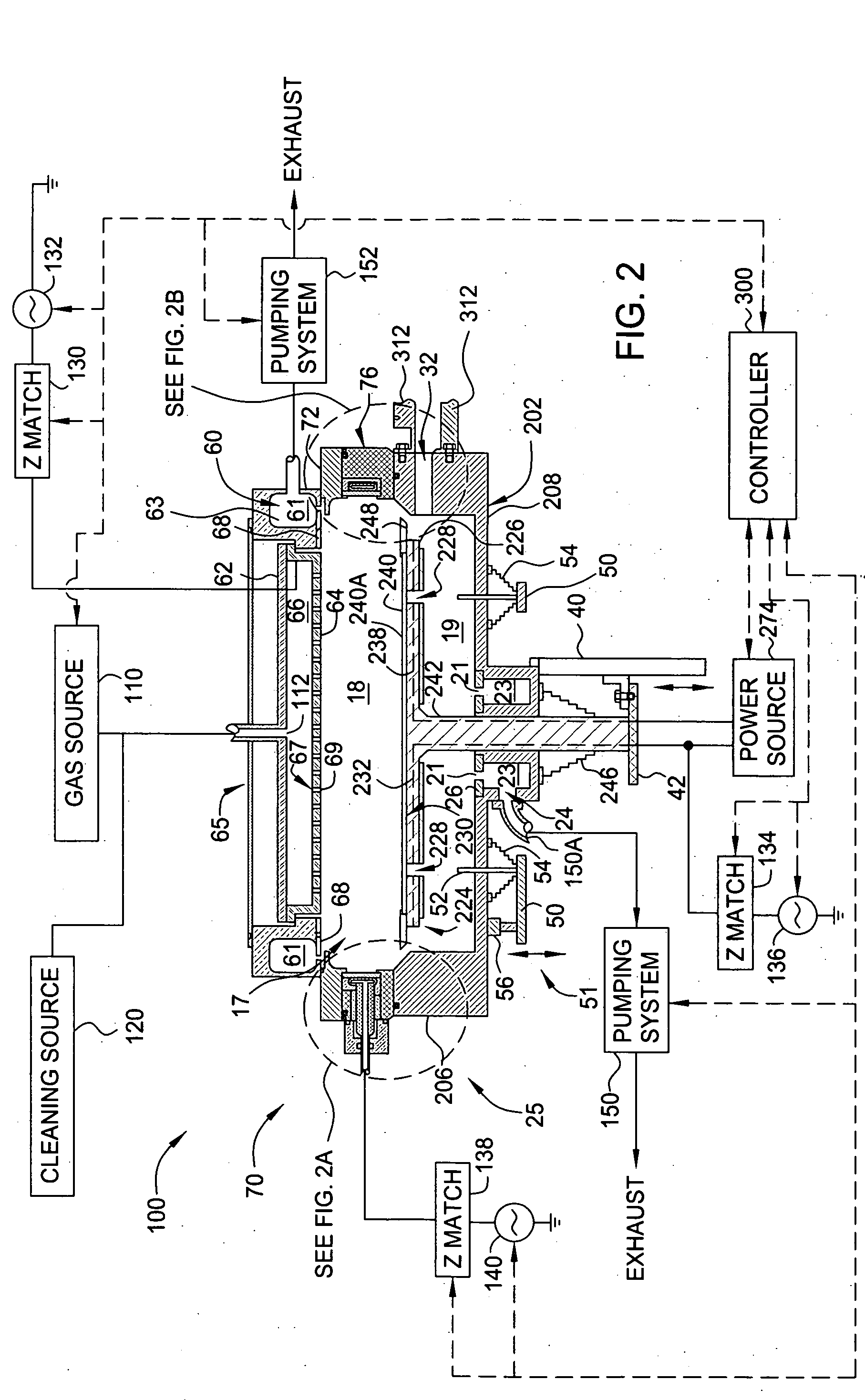
[0028] The present invention generally provides an apparatus and method for processing a surface of a substrate using an inductively coupled high density plasma. In general, aspects of the present invention can be used for flat panel display processing, semiconductor processing, solar cell processing, or any other substrate processing. The invention is illustratively described below in reference to a chemical vapor deposition system, processing large area substrates, such as a plasma enhanced chemical vapor deposition (PECVD) system, available from AKT, a division of Applied Materials, Inc., Santa Clara, Calif. However, it should be understood that the apparatus and method may have utility in other system configurations, including those systems configured to process round substrates.

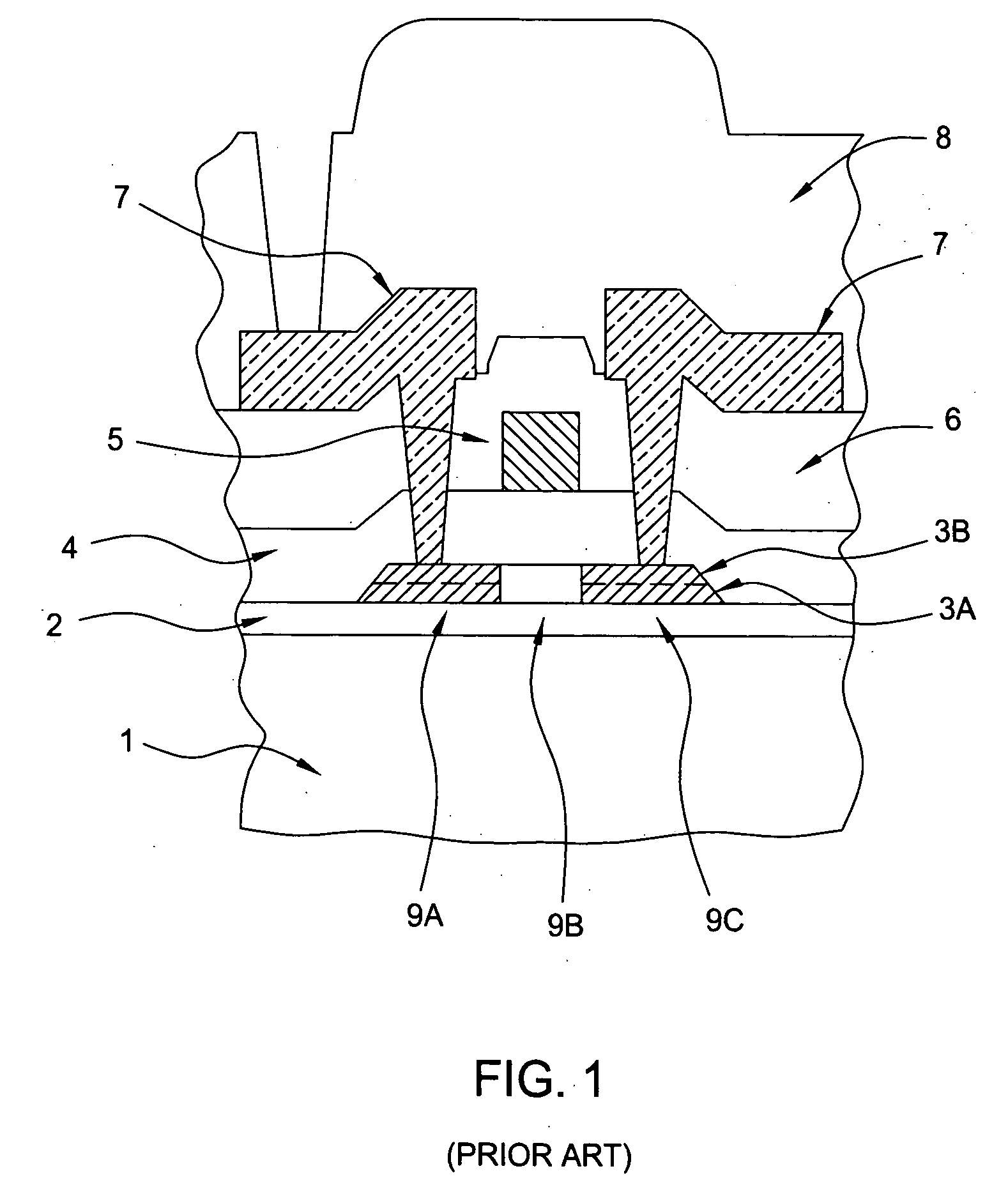
[0029]FIG. 1 illustrates a cross-sectional schematic view of a thin film transistor structure. The optically transparent optically transparent substrate 1 may comprise a material that is essentially opt...


PUM

PropertyMeasurementUnit
Temperatureaaaaaaaaaa
Thicknessaaaaaaaaaa

Abstract

A method and apparatus that is useful for forming a high quality gate dielectric layer in MOS TFT devices using a high density plasma oxidation (HDPO) process. The HDPO process forms a good interface and then a second layer, which has good bulk electrical properties, is deposited at a higher deposition rate over the HDPO layer. In one embodiment a thin HDPO process layer is formed over the channel, source and drain regions to form a high quality dielectric interface and then one or more dielectric layers are deposited on the HDPO layer to form a high quality gate dielectric layer. The HDPO process generally entails using an inductively and/or capacitively coupled RF energy transmitting device to generate and control the plasma generated over the surface of the substrate and injecting a gas containing an oxidizing source to grow the interfacial layer. A second dielectric layer may then be deposited on the surface of the substrate using a CVD or plasma enhanced CVD deposition process. Aspects of the present invention also provide a cluster tool that contains at least one specialized plasma processing chamber that is capable of depositing a high quality gate dielectric layer. The cluster tool is advantageous because it supports both the pre-processing steps, such as, preheating the substrate, pre-cleaning the surface of the substrate prior to processing, and cool down after processing, all in a single controlled environment.

Description

BACKGROUND OF THE INVENTION [0001] 1. Field of the Invention [0002] Embodiments of the present invention generally relate to an apparatus and method used for fabricating electronic devices using a plasma processing system. [0003] 2. Description of the Related Art [0004] In the fabrication of flat panel displays (FPD), thin film transistors (TFT) and liquid crystal cells, metal interconnects and other features are formed by depositing and removing multiple layers of conducting, semiconducting and dielectric materials on a glass substrate. The various features formed are integrated into a system that collectively is used to create, for example, active matrix display screens in which display states are electrically created in individual pixels on the FPD. Processing techniques used to create the FPD include plasma-enhanced chemical vapor deposition (PECVD), physical vapor deposition (PVD), etching, and the like. Plasma processing is particularly well suited for the production of flat p...

Claims


Application Information

Patent Timeline
IPC IPC(8): C23C16/00H05H1/24
CPCC23C8/36C23C16/0218C23C16/402C23C16/50C23C16/00
Inventor WHITE, JOHN M.
Owner APPLIED MATERIALS INC
Why Eureka
Try Eureka