Apparatus and circuit for power supply, and apparatus for controlling large current load

a technology of power supply and circuit, applied in the direction of electric variable regulation, process and machine control, instruments, etc., can solve the problems of power semiconductor device thermal destruction, power semiconductor device switching loss, and temperature rise of the power semiconductor device itsel

Inactive Publication Date: 2006-06-01
FURUKAWA ELECTRIC CO LTD
View PDF7 Cites 24 Cited by
  • Summary
  • Abstract
  • Description
  • Claims
  • Application Information

AI Technical Summary

Benefits of technology

[0035] A power supply apparatus according to one aspect of the present invention includes a diode that is disposed in the path of a main current that is a subject of power control. The diode includes: a substrate; a gallium-nitride buffer layer formed on the substrate; a gallium-nitride layer formed on the gallium-nitride buffer layer; and an n-type aluminum-gallium-nitride layer formed on the gallium-nitride layer.
[0036] A power supply circuit according to another aspect of the present invention has a transformer, and conducts on / off control on voltage applied to a primary winding of said transformer, and thereby supplies a stabilized power supply voltage to a secondary winding side of said transformer. The power supply circuit includes a GaN-diode that includes: a substrate; a gallium-nitride buffer layer formed on the substrate; a gallium-nitride layer formed on the gallium-nitride buffer layer; and an n-type aluminum-gallium-nitride layer formed on the gallium-nitride layer. The GaN-diode is connected to the secondary winding of said transformer and on / off-controlled by a gate signal.

Problems solved by technology

In these power semiconductor devices, there are switching loss caused by superposition of transient voltage and current at the time of switching and conduction loss caused at the time of conduction.
Heat generated by the power semiconductor device causes a temperature rise of the power semiconductor device itself.
As a result, thermal destruction of the power semiconductor device is caused by thermal runaway.
This results in a problem that the whole power supply apparatus becomes large in weight and capacity.
Because of installation of the radiator 302, the weight and volume of the whole power supply apparatus become excessively large.
This brings about limitation on design that the radiator needs to be disposed with due regard to the outer periphery of the casing of the power supply apparatus and the radiation path.
This results in a problem that the degree of freedom of the power supply apparatus is reduced.
Thus, there is also a problem that the design of the whole device is largely affected.
This results in a problem that much time and labor are required for radiation design and arrangement design of other circuit elements included in the power supply apparatus.
When the temperature has risen to a predetermined value, the heat protection circuit conducts fail safe control, such as stopping the power supply apparatus and causing shift to a low dissipation mode.
This heat protection circuit is a complicated circuit that senses the temperature, output current, and so on and conducts a shift to fail safe control by using a logic processing circuit.
Thus, there is a problem that the power supply apparatus must have a heat protection circuit having such a complicated circuit.
As a result, the conventional power supply circuit has a problem that the circuit configuration becomes large and heavy because of the radiation plate.
In this control apparatus, however, the power MOS-FET used as the switching element of on / off control generates much heat.
As a result, the conventional large load control apparatus has a problem that the circuit configuration becomes large and heavy because of the radiation plate.

Method used


Image

  • Apparatus and circuit for power supply, and apparatus for controlling large current load
  • Apparatus and circuit for power supply, and apparatus for controlling large current load
  • Apparatus and circuit for power supply, and apparatus for controlling large current load

Examples


first embodiment

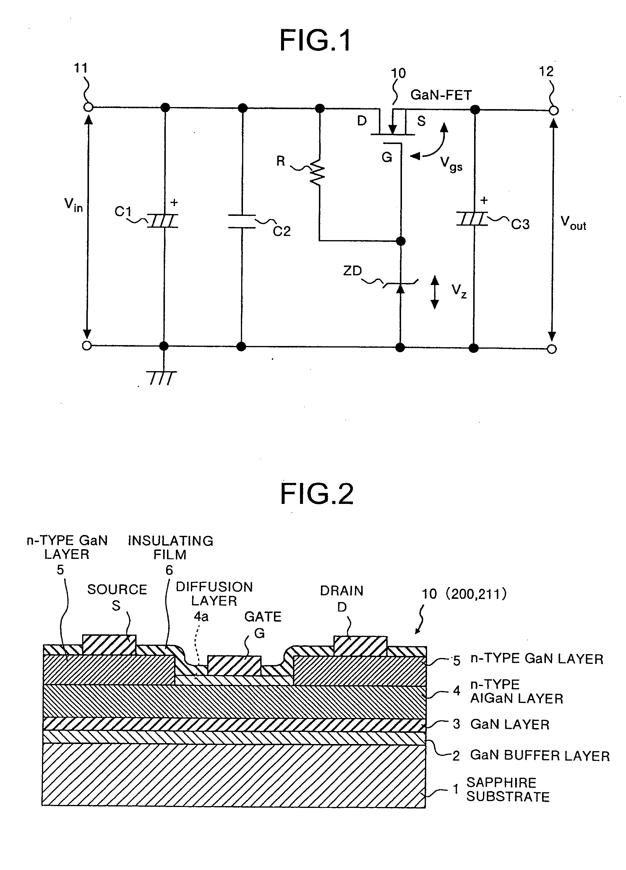
[0058]FIG. 1 is a diagram showing a schematic circuit configuration of the power supply apparatus according to the present invention. This power supply apparatus is a linear regulator. This power supply apparatus is a stabilized power supply apparatus for converting an input voltage Vin of 12 VDC to 5VDC of maximum 10 A and outputting the 5VDC as an output voltage Vout.

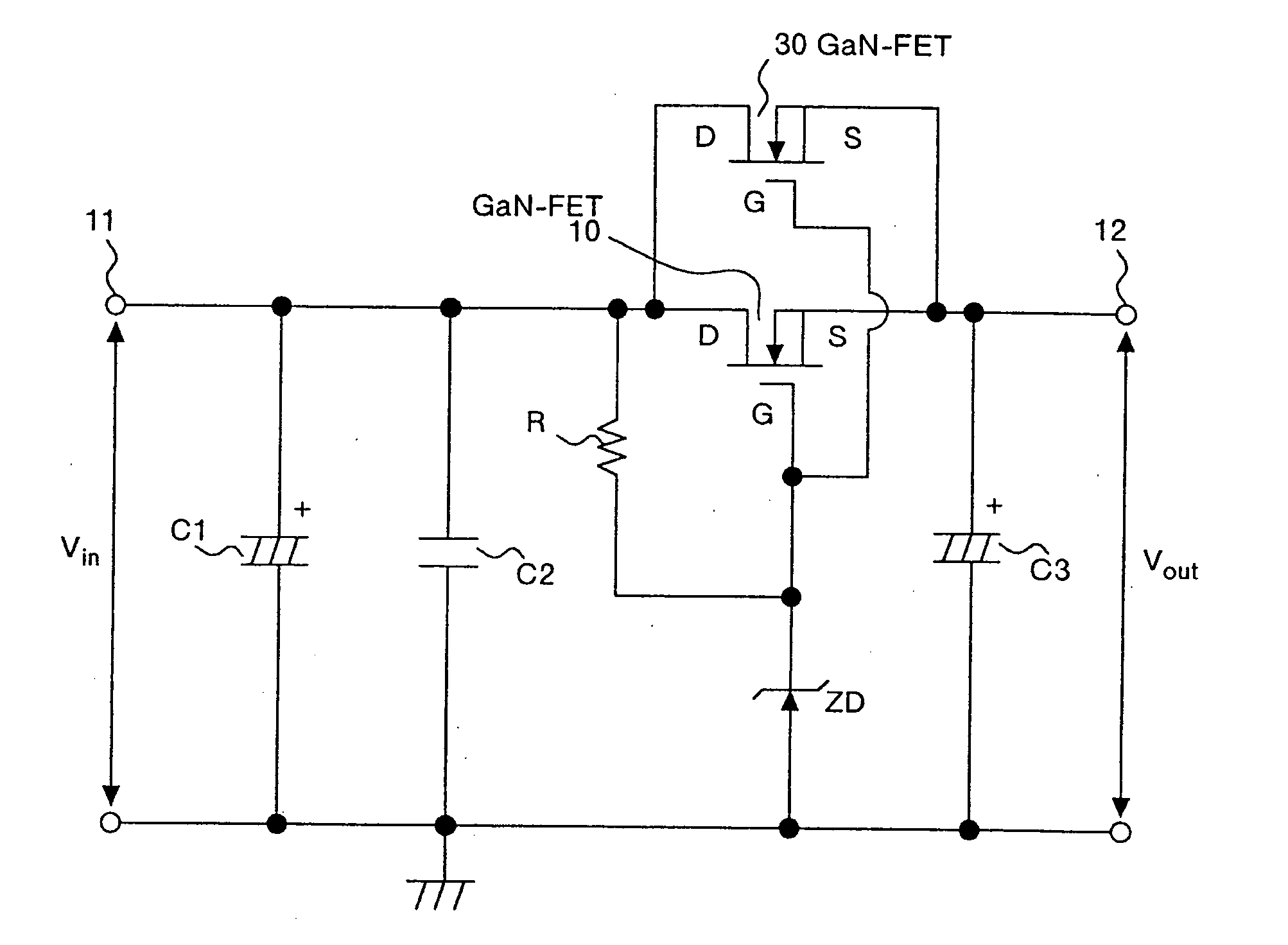
[0059] In FIG. 1, a GaN-FET 10 is connected between an input terminal 11 of an input voltage Vin side and an output terminal 12 of an output voltage Vout side. Drain D and source S of the GaN-FET 10 are connected to the input terminal 11 side and the output terminal 12 side, respectively. Gate G of the GaN-FET 10 is connected to a Zener diode ZD. In other words, the GaN-FET 10 controls the main current, which flows from the input voltage Vin side to the output terminal Vout side.

[0060] An electrolytic capacitor C1 is a capacitor for smoothing a voltage waveform in the case where the input voltage Vin is full-wave rec...

third embodiment

[0092]FIG. 7 is a diagram showing a schematic circuit configuration of another power supply apparatus that is the present invention. Although the power supply apparatus shown in FIG. 6 is a switching regulator of forward type, the power supply apparatus shown in FIG. 7 is a switching regulator of flyback type. In other words, in the power supply apparatus shown in FIG. 6, power energy of the primary side is transferred to the secondary side when the GaN-FET 40 is on. In the power supply apparatus shown in FIG. 7, power energy of the primary side is transferred to the secondary side when a GaN-FET 50 is off.

[0093] With reference to FIG. 7, in this switching regulator, a pulse width modulation (PWM) signal output by a pulse width control circuit 51 is applied to the GaN-FET 50 at its gate, and the GaN-FET 50 is switched. A winding direction of a transformer T2 is different from a winding direction of a transformer T1. When the GaN-FET 50 is on, energy of an input voltage Vin is stored...

fourth embodiment

[0103]FIG. 9 is a diagram showing a schematic circuit configuration of a power supply apparatus that is the present invention. The power supply apparatus shown in FIG. 9 rectifies an AC current supplied from a commercial three-phase AC power source 90, by using a diode group included in a rectifying circuit 91, and smooths the rectified current by using an electrolytic capacitor C91. The smoothed current is converted to an AC current having a desired frequency and a desired output voltage by an inverter circuit 92. The AC current is output to an induction motor (IM) 94.

[0104] The inverter circuit 92 includes GaN-FET pairs 101 and 102, 103 and 104, and 105 and 106 serving as switching element pairs respectively corresponding to the U phase, V phase and W phase. A drive control section 93 sends PWM signals corresponding to respective phases to the GaN-FET pairs 101 to 106, and conducts switching control on each of each of the GaN-FET pairs 101 to 106, and three-phase AC power having a...


PUM


Abstract

A power supply apparatus includes a diode that is disposed in the path of a main current that is a subject of power control. The diode includes a substrate; a gallium-nitride buffer layer formed on the substrate; a gallium-nitride layer formed on the gallium-nitride buffer layer; and an n-type aluminum-gallium-nitride layer formed on the gallium-nitride layer.

Description

CROSS-REFERENCE TO RELATED APPLICATIONS [0001] This application is a continuation-in-part of U.S. co-pending patent application Ser. No. 10 / 917,346, filed Aug. 13, 2004, now abandoned, which is a continuation of U.S. patent application Ser. No. 09 / 926,281, filed Oct. 23, 2001, now U.S. Pat. No. 6,861,828. The priority of these prior applications is expressly claimed and their disclosures are hereby incorporated by reference in their entirety.BACKGROUND OF THE INVENTION [0002] 1. Field of the Invention [0003] The present invention relates to various power supply apparatuses used in automobiles, electric vehicles, construction machinery, various public welfare devices (such as video devices, television sets, and audio devices), various industrial devices (such as personal computers, communication devices, and FA control devices), and so on. Furthermore, the present invention relates to a power supply circuit and a large current load control apparatus of switching power supply using Ga...

Claims


Application Information

Patent Timeline
Patent Type & Authority Applications(United States)
IPC IPC(8): G05F1/56
CPCH01L29/2003H01L29/7787H02M3/00H02M7/003Y02B70/1483Y02B70/10H02M3/003
Inventor WATANABE, YUICHIIIJIMA, TAKASHI
Owner FURUKAWA ELECTRIC CO LTD
Why Eureka
Try Eureka