Design method and architecture for power gate switch placement

a technology of design method and architecture, applied in logic circuit coupling/interface arrangement, pulse technique, instruments, etc., to achieve the effect of avoiding performance penalties and not increasing the overall real estate requirement of the integrated circui

Active Publication Date: 2006-06-01
ANSYS
View PDF6 Cites 24 Cited by
  • Summary
  • Abstract
  • Description
  • Claims
  • Application Information

AI Technical Summary

Benefits of technology

[0015] In one embodiment, power-gated logic cells are placed along with non-power-gated logic cells (i.e., logic cells that are directly connected to the true ground voltage reference). The non-power-gated logic cells may be used to achieve higher circuit performance where needed. In this manner, high circuit performance is achieved while trading-off a very small amount of additional leakage current.
[0016] In one embodiment, the unoccupied spaces into which power gate cells are placed occur at a more or less random fashion, so that the power gate cells are placed in a more or less irregular distribution. Optimization techniques may be applied to reduce the irregularity of the distribution of the power gate cells. Such optimization techniques may include adjusting the number of power gate cells to use, the size of each power gate cell and the selected locations of the power gate cells.

Problems solved by technology

Leakage currents flow in logic circuits from a power supply node into the ground node because the switching characteristics of the transistors in the logic circuits are not ideal (i.e., the transistors cannot be completely shut off).

Method used


Image

  • Design method and architecture for power gate switch placement
  • Design method and architecture for power gate switch placement
  • Design method and architecture for power gate switch placement

Examples


Embodiment Construction

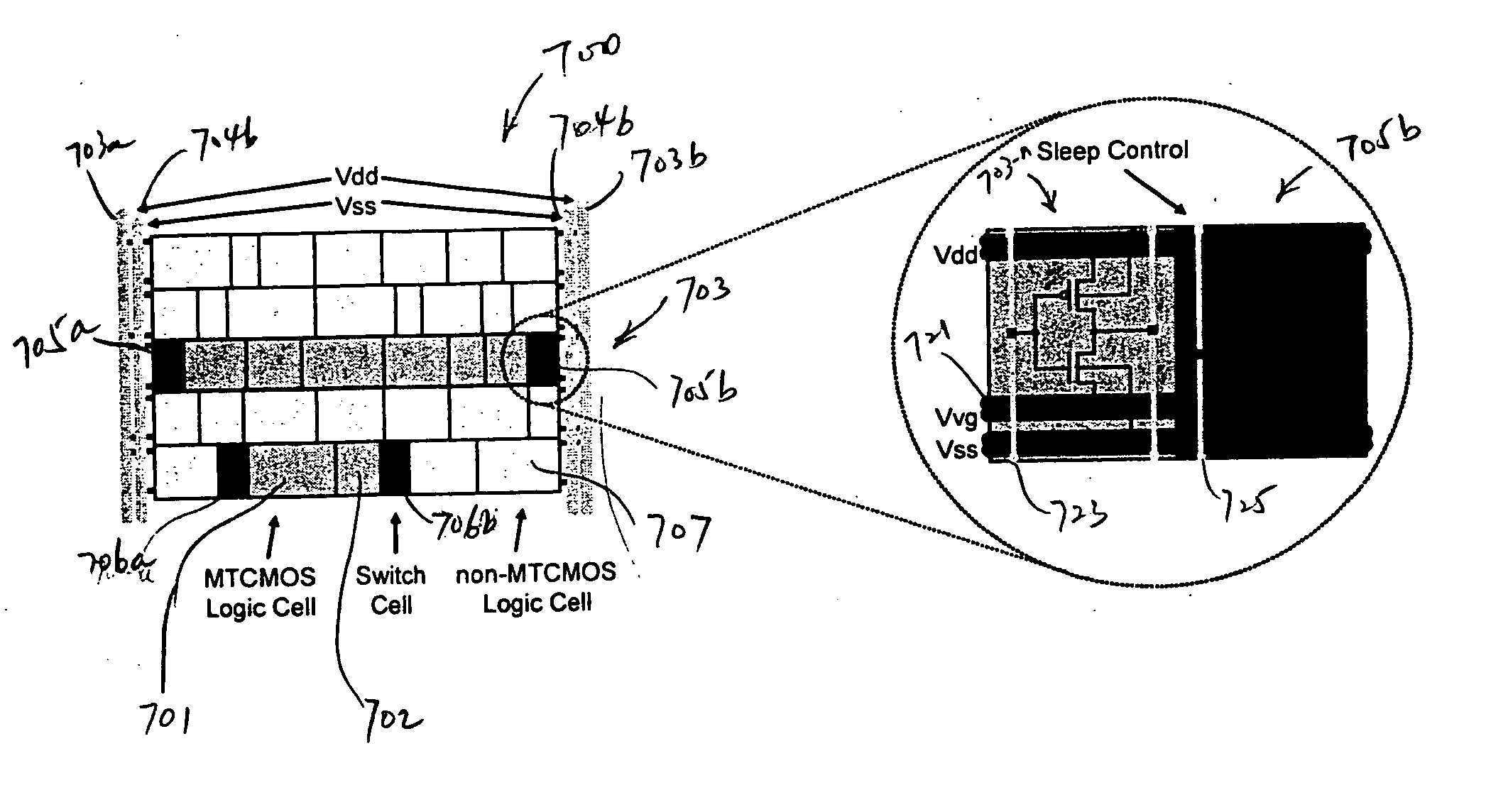
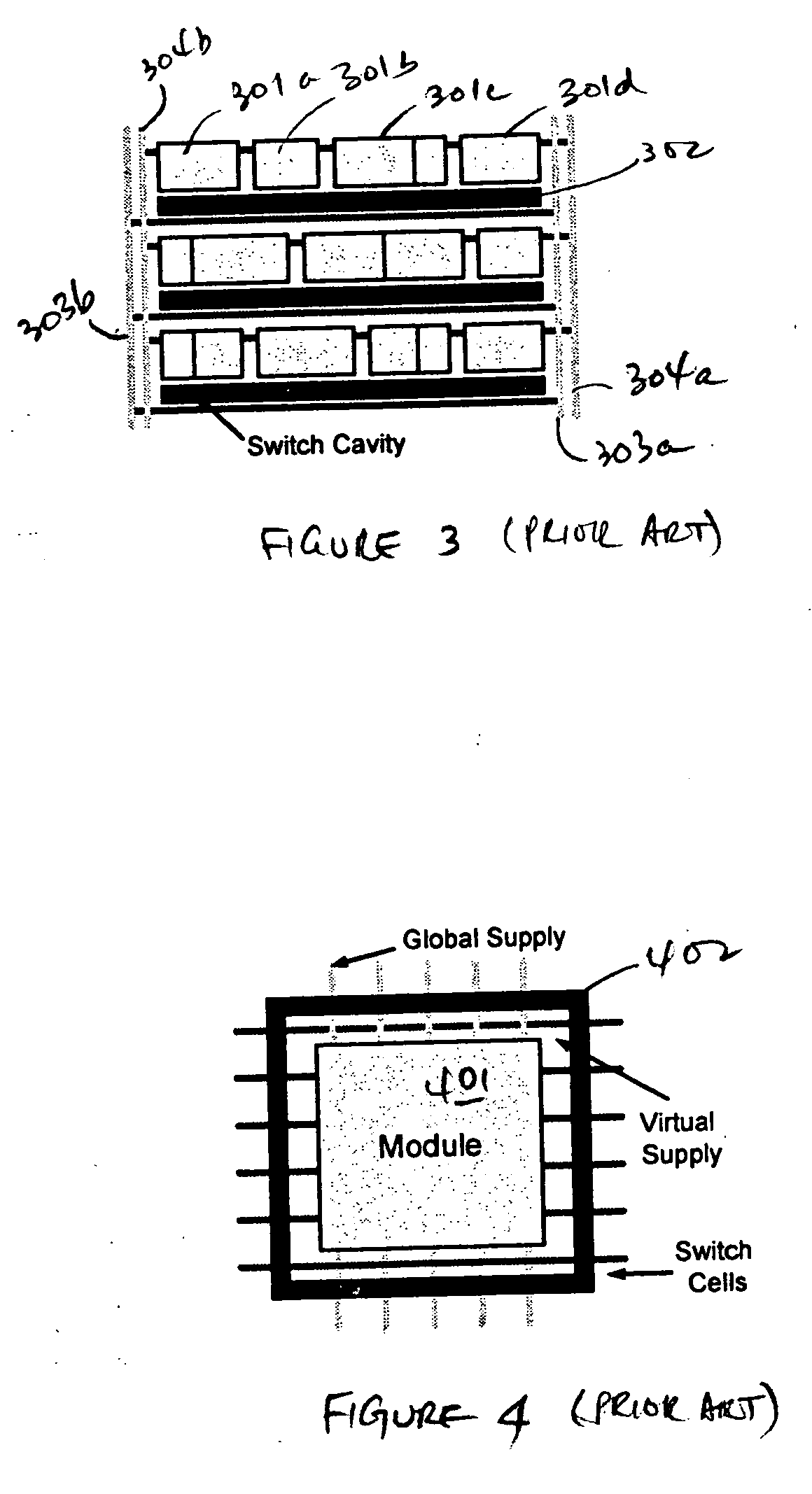
[0030] The present invention provides a design method in which power gates or switch cells are placed at unoccupied locations of logic cell rows. The inventors observe that, using conventional standard cell design and placement techniques, the placement density or utilization that can be achieved is typically between 70-80% (i.e., unoccupied space constitutes between 20 to 30% of the available space in each row of logic cells). The present invention places power gate cells in the unoccupied space. The available unoccupied space typically provides sufficient space to accommodate all the power gate cells required in a row of logic cells. Thus, inclusion of power gates in the logic circuit design does not increase the silicon real estate requirement.

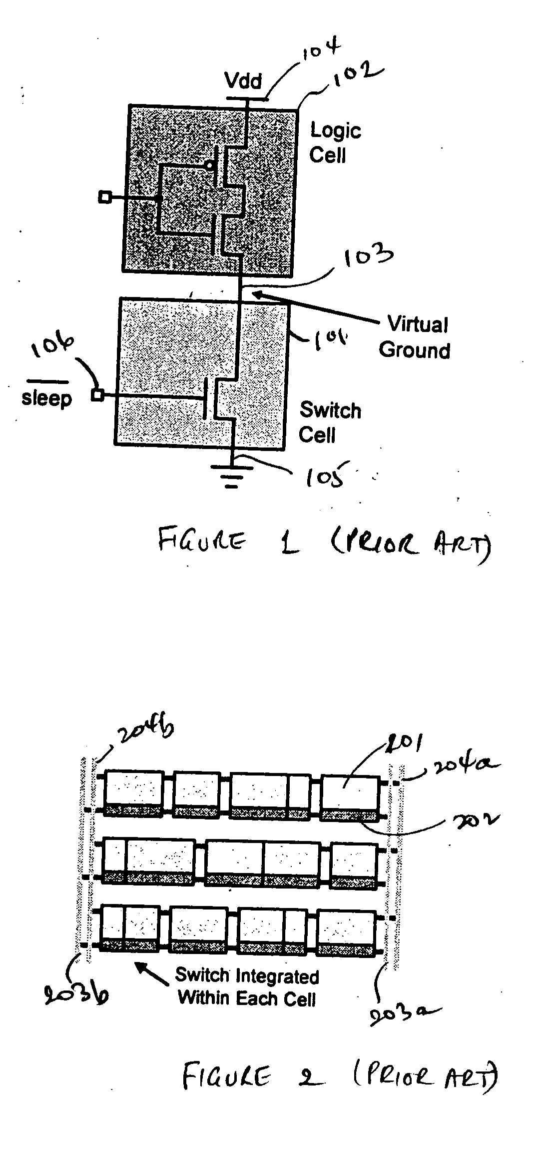
[0031] In this detailed description, the present invention is illustrated by embodiments in which the power gate cells connect the logic cells to a true ground voltage reference. However, the present invention is equally applicable to powe...


PUM


Abstract

A design method places power gates or switch cells using unoccupied locations of logic cell rows. Two types of such switch cells, filler switches and sealer switches, may be provided using the unoccupied locations. In one embodiment, virtual ground voltage references to the logic cells are routed to their associated switch cells. Because conventional standard cell design and placement techniques achieve only a placement density or utilization between 70-80% (i.e., unoccupied space constitutes between 20 to 30% of the available space in each row of logic cells), by placing the power gate cells in the unoccupied space, the method does not increase the silicon real estate requirement even though the power gate cells are introduced into the design. Optimization techniques may be applied to achieve proper sizing and distribution of power gate cells, so as to avoid a performance penalty due to the power gate cells. In one embodiment, fine-grained power gating is achieved by selectively providing non-power-gated logic cells among power-gated logic cells.

Description

BACKGROUND OF THE INVENTION [0001] 1. Field of the Invention [0002] The present invention relates to a method for designing multi-threshold complementary metal-oxide-semiconductor (MTCMOS) circuits and the physical architecture of the circuits resulting from using such a method. In particular, the present invention relates to a design method for placing power switches in an MTCMOS circuit, and the physical circuit architecture of MTCMOS circuits resulting from using this method. [0003] 2. Discussion of the Related Art [0004] A significant concern in integrated circuit design is reducing leakage currents. Leakage currents flow in logic circuits from a power supply node into the ground node because the switching characteristics of the transistors in the logic circuits are not ideal (i.e., the transistors cannot be completely shut off). [0005] In MTCMOS circuits, one technique that reduces leakage current is to a place a “power gate” (also known as “power switch” or simply, “switch cel...

Claims


Application Information

Patent Timeline
Patent Type & Authority Applications(United States)
IPC IPC(8): H03K19/23H03K19/0175
CPCG06F17/5031G06F17/5068G06F17/5077H01L27/0207H01L27/11807H03K19/0016G06F30/3312G06F30/394G06F30/39G06F30/3947G06F30/347
Inventor FRENKIL, GERALD L.VENKATRAMAN, SRINIVASAN
Owner ANSYS
Why Eureka
Try Eureka