Solder interconnect on IC chip

a technology of ic chips and soldering, applied in the direction of semiconductor devices, semiconductor/solid-state device details, electrical devices, etc., can solve the problems of large nosie, high signal transmission efficiency, computation errors, etc., and achieve the effect of enhancing electrical performan

Active Publication Date: 2006-06-15
QUALCOMM INC
View PDF99 Cites 28 Cited by
  • Summary
  • Abstract
  • Description
  • Claims
  • Application Information

AI Technical Summary

Benefits of technology

[0006] The first objective of the invention is to provide a semiconductor chip with a bump enhancing the electrical performance ...

Problems solved by technology

The wirebonded conducting wire has a small cross-sectional area vertical to the direction of signal transmission which causes unexpected large nosie, and worse, computation errors.
In fact, according to t...

Method used


Image

  • Solder interconnect on IC chip
  • Solder interconnect on IC chip
  • Solder interconnect on IC chip

Examples


first embodiment

1. First Embodiment of Chip Packages

[0069] In the first embodiment, the chip is bonded to a circuit of a substrate by bumps wherein the bumps can be bonded to the substrate by soldering bonding or Au—Au Eutectic Bonding. Here, some feasible examples are described as follows.

[0070] 1.Bump on thin-film circuit or passivation layer of semiconductor chip being bonded to circuit layer of substrate.

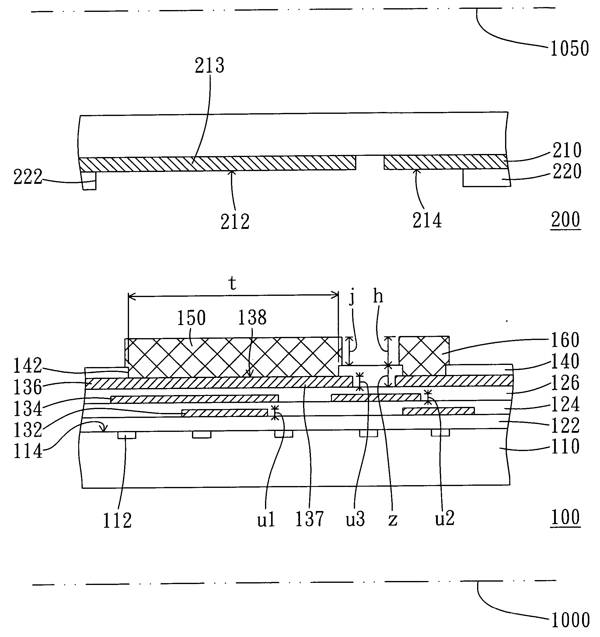
[0071]FIG. 1 is a cross-sectional view showing a chip package before a semiconductor chip and substrate being assembled according to a first embodiment. A semiconductor chip 100 includes a semiconductor substrate 110, multiple thin-film dielectric layers 122, 124 and 126, multiple thin-film circuit layers 132, 134 and 136, and a passivation layer 140.

[0072] Referring to FIG. 1, the semiconductor substrate 110 has multiple electronic elements 112 in a surface layer of an active surface 114 of the semiconductor substrate 110. The semiconductor substrate 110 could be a silicon substrate. By dop...

second embodiment

2. Second Embodiment of Chip Packages

[0250] The bumps not only can bond a semiconductor chip to a substrate but also can bond two semiconductor chips, as shown in the following FIG. 29-51. The structure of the semiconductor chips has been described in the first embodiment and the related description is omitted hereinafter. Some embodiments are described as follows.

[0251] 1.Bump on thin-film circuit of a semiconductor chip being bonded to another bump on passivation layer or thin-film circuit of another chip

[0252] FIGS. 29 is a cross-sectional views showing a chip package before two semiconductor chips being assembled according to a second embodiment. FIG. 30 is a cross-sectional view showing a chip package created after bonding two semiconductor chips shown in FIG. 29.

[0253] Referring to FIG. 29, a semiconductor chip 300 includes a semiconductor substrate 310, multiple thin-film dielectric layers 322, 324 and 326, multiple thin-film circuit layers 332, 334 and 336, and a passivat...

third embodiment

3. Third Embodiment of Chip Packages

[0400] In the previous embodiments, the bumps 150 and 160 are joined to substrate 200 or semiconductor chip 300 by soldering or Au—Au eutectic bonding. Alternatively, the bumps 150 and 160 can be electrically connected to a substrate 400 through a conductive layer 450 with polymer 452 and multiple metal particles 454, as shown in FIGS. 52-56. The structure of the semiconductor chip 100 can refer to that described in the first embodiment. The substrate 400 could be a glass substrate, a ceramic substrate, or a substrate composed of multiple polymer layers. FIGS. 52-56 show a substrate taking an example of a glass substrate including a transparent circuit layer 410, such as ITO (Indium Tin Oxide). Some feasible embodiments are described as follows.

[0401] 1.Bump on thin-film circuit or passivation layer of semiconductor chip being bonded to circuit layer of glass substrate through metal particles in conductive layer

[0402]FIG. 52 is a cross-sectional...


PUM


Abstract

A semiconductor chip suited for being electrically connected to a circuit element includes a line and a bump. The bump is connected to the line and is adapted to be electrically connected to the line. A plane that is horizontal to an active surface of the semiconductor chip is defined. The area that the connection region of the line and the bump is projected on the plane is larger than 30,000 square microns or has an extension distance larger than 500 microns.

Description

BACKGROUND OF THE INVENTION [0001] 1. Field of the Invention [0002] This invention relates to a semiconductor chip, chip package and package process, and particularity to ones with high performance. [0003] 2. Description of the Related Art [0004] As the tremendous development of IT (Information Technology) proceeds, it's always been a piece of cake for retrieving information far away from us. Also, with the aid of high-efficiency IT product, enterprise competitor would be of benefit taking the lead in the game of time. IT product constantly renews itself and integrates various circuit designs, resulting in bearing much more function in just one chip. Moreover, plus the advanced technology of semiconductor, the success of mass production for IC copper process and the integrating of circuits, most signal transmission can be done in the same chip. Therefore, reduction of signal transmitting path will bring the high effiency of chip. [0005] After completing the desired chip, it is then ...

Claims


Application Information

Patent Timeline
IPC IPC(8): H01L23/48
CPCH01L23/528H01L24/10H01L24/13H01L25/0657H01L2224/13099H01L2225/06513H01L2924/01005H01L2924/01013H01L2924/01015H01L2924/01022H01L2924/01029H01L2924/01049H01L2924/01073H01L2924/01074H01L2924/01079H01L2924/01082H01L2924/01322H01L2924/04941H01L2924/04953H01L2924/09701H01L2924/12044H01L2924/14H01L2924/01006H01L2924/01019H01L2924/01023H01L2924/01024H01L2924/01033H01L2924/01047H01L2924/014H01L2224/16106H01L24/81H01L2924/00H01L2924/15787H01L2924/15788H01L2224/81805H01L2224/13H01L2224/05567H01L2224/05573H01L2224/05624H01L2224/05647H01L2224/06167H01L24/14H01L24/16H01L24/17H01L2224/0603H01L2224/06051H01L2224/1403H01L2924/00014H01L2224/0554H01L2224/05599H01L2224/0555H01L2224/0556
Inventor LIN, MOU-SHIUNG
Owner QUALCOMM INC
Why Eureka
Try Eureka