Nitride semiconductor light-emitting device and method for producing same

a technology of nitride semiconductor and light-emitting device, which is applied in the direction of semiconductor lasers, solid-state devices, lasers, etc., can solve the problems of low yield rate, no great improvement in yield rate, cracking, etc., and achieves high yield rate, inhibit cracking, good surface flatness

Active Publication Date: 2006-06-22
SHARP FUKUYAMA LASER CO LTD
View PDF8 Cites 38 Cited by
  • Summary
  • Abstract
  • Description
  • Claims
  • Application Information

AI Technical Summary

Benefits of technology

[0025] By using the present invention, nitride semiconductor grown layers with good surface flatness and inhibited cracking are formed over the nitride semiconductor substrate. This enables it to obtain highly reliable nitride semiconductor light-emitting devices at a high yield rate.

Problems solved by technology

One of the causes that have kept the yield rate low is the occurrence of cracking.
However, when the above-described processed substrate was used and nitride compound semiconductors were grown over the substrate by the MOCVD (Metal Organic Vapor Deposition) method or the like to prepare a semiconductor laser device, occurrence of cracking was prevented, but no great improvement in the yield rate was obtained.
Thus, if concaves (grooves) remain on a nitride compound semiconductor, the concaves cause deterioration of the flatness of the film.
It is considered that the deteriorated flatness in turn causes variation of thickness of each layer of the device and chip-to-chip fluctuation of characteristics, resulting in a deteriorated yield rate.

Method used


Image

  • Nitride semiconductor light-emitting device and method for producing same
  • Nitride semiconductor light-emitting device and method for producing same
  • Nitride semiconductor light-emitting device and method for producing same

Examples


Embodiment Construction

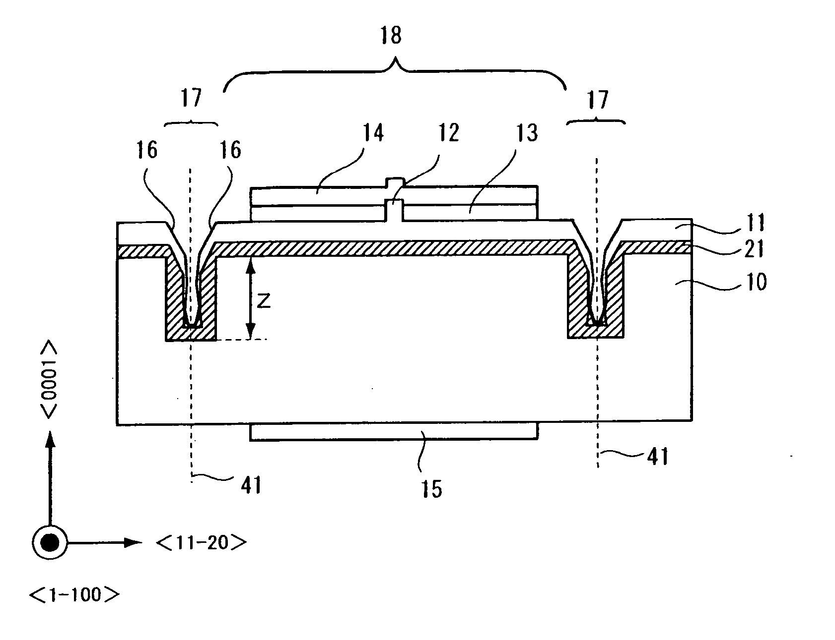
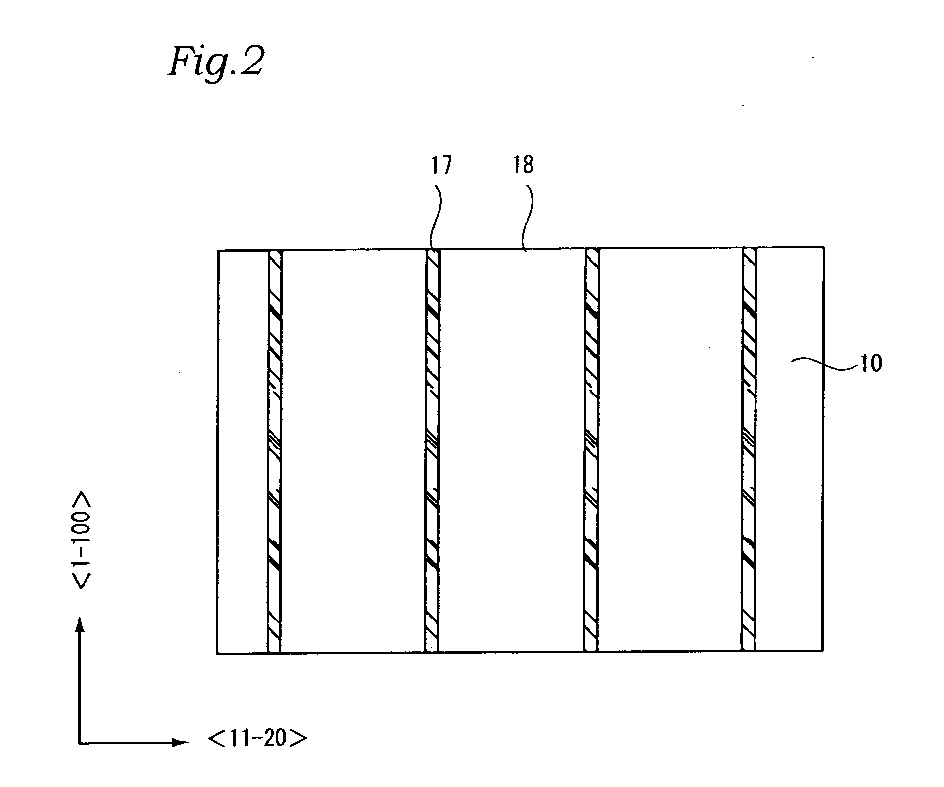
[0034] Preparation of nitride semiconductor grown layers with good surface flatness and inhibited cracking over a nitride semiconductor substrate, which is an object of the present invention, has been realized by preparing a nitride semiconductor substrate having stripe groove portions, and by forming an underlying layer having nitride semiconductor on the nitride semiconductor substrate including the side walls of the groove portions, in such a manner that the underlying layer has a crystal surface in each of the groove portions and the crystal surface is tilted at an angle of from 53.5° to 63.4° with respect to the surface of the substrate.

[0035] First, the meanings of terms used in this specification will be clarified in advance.

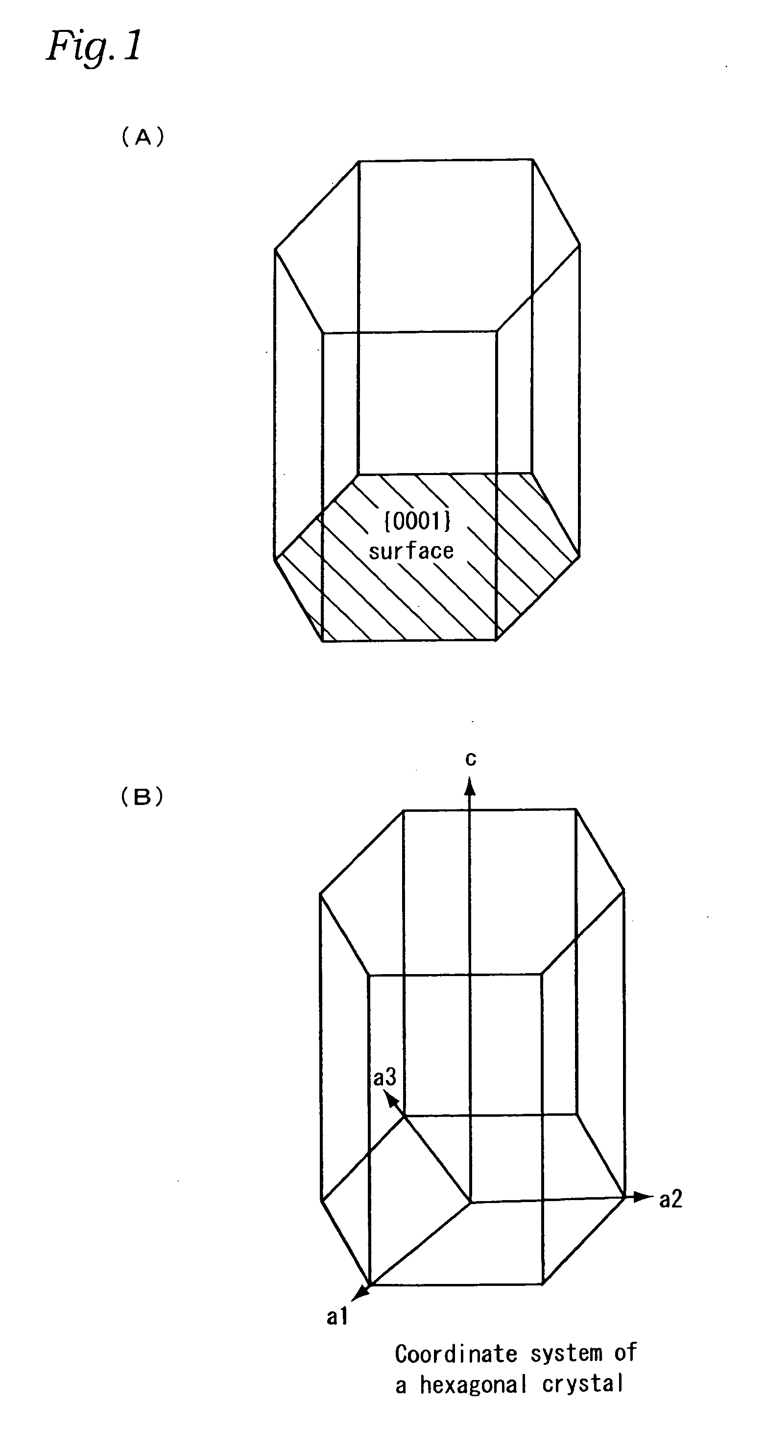
[0036] The term “nitride semiconductor substrate” can be any substrate that is made of nitride semiconductor, examples including a AlaGabIncN (0≦a≦1, 0≦b≦1, 0≦c≦1, a+b+c=1) substrate. It is also possible that approximately 10% or less of the nitrogen el...


PUM

PropertyMeasurementUnit
angleaaaaaaaaaa
thicknessaaaaaaaaaa
depthaaaaaaaaaa

Abstract

In a method for producing a nitride semiconductor light-emitting device according to the present invention, first, a nitride semiconductor substrate having groove portions formed is prepared. An underlying layer comprising nitride semiconductor is formed on the nitride semiconductor substrate including the side walls of the groove portions, in such a manner that the underlying layer has a crystal surface in each of the groove portions and the crystal surface is tilted at an angle of from 53.5° to 63.4° with respect to the surface of the substrate. Over the underlying layer, a light-emitting-device structure composed of a lower cladding layer containing Al, an active layer, and an upper cladding layer containing Al is formed. According to the present invention, thickness nonuniformity and lack of surface flatness, which occur when accumulating a layer with light-emitting-device structure of nitride semiconductor over the nitride semiconductor substrate, are alleviated while inhibiting occurrence of cracking.

Description

BACKGROUND OF THE INVENTION [0001] The present invention relates to a method for producing a nitride semiconductor light-emitting device, and more particularly to a method for producing a nitride semiconductor light-emitting device improved to prevent cracking and obtain nitride semiconductors and nitride semiconductor laser devices at a high yield rate. The present invention also relates to a nitride semiconductor light-emitting device obtained by such a method. [0002] By using nitride semiconductor crystals represented by GaN, AlN, InN, and mixed crystals thereof, semiconductor laser devices that oscillate in the ultraviolet-visible region are being produced. As the substrate, a GaN substrate is often used and being studied with vigor in associated research institutions. Currently, the yield rate of semiconductor laser devices (e.g., the rate of good products obtained from one wafer) is significantly low, and improvement is highly necessary for cost reduction and the like. One of ...

Claims


Application Information

Patent Timeline
Patent Type & Authority Applications(United States)
IPC IPC(8): H01L21/00H01L33/00H01S5/22H01S5/343
CPCB82Y20/00H01L33/007H01S5/0202H01S5/0207H01S5/0211H01S5/0425H01S5/2201H01S5/2214H01S5/3202H01S5/34333H01S5/320225H01S5/04254H01S2301/176
Inventor TAKAKURA, TERUYOSHIITO, SHIGETOSHIKAMIKAWA, TAKESHI
Owner SHARP FUKUYAMA LASER CO LTD
Why Eureka
Try Eureka