Repairable three-dimensional semiconductor subsystem

a three-dimensional semiconductor and subsystem technology, applied in semiconductor devices, semiconductor/solid-state device details, electrical devices, etc., can solve the problems of buckling, cracking or delamination, shear force at the interface between the chip and the substrate, and non-compliant, and achieves low thermal impedance and superior thermal performance.

Active Publication Date: 2006-06-22
IP3 2022 SERIES 922 OF ALLIED SECURITY TRUST I
View PDF99 Cites 39 Cited by
  • Summary
  • Abstract
  • Description
  • Claims
  • Application Information

AI Technical Summary

Benefits of technology

[0014] One or more of the integration platforms may include an interface adaptor for superior thermal performance (low thermal impedance from junction to case, θJC). The interface adaptor is prefera

Problems solved by technology

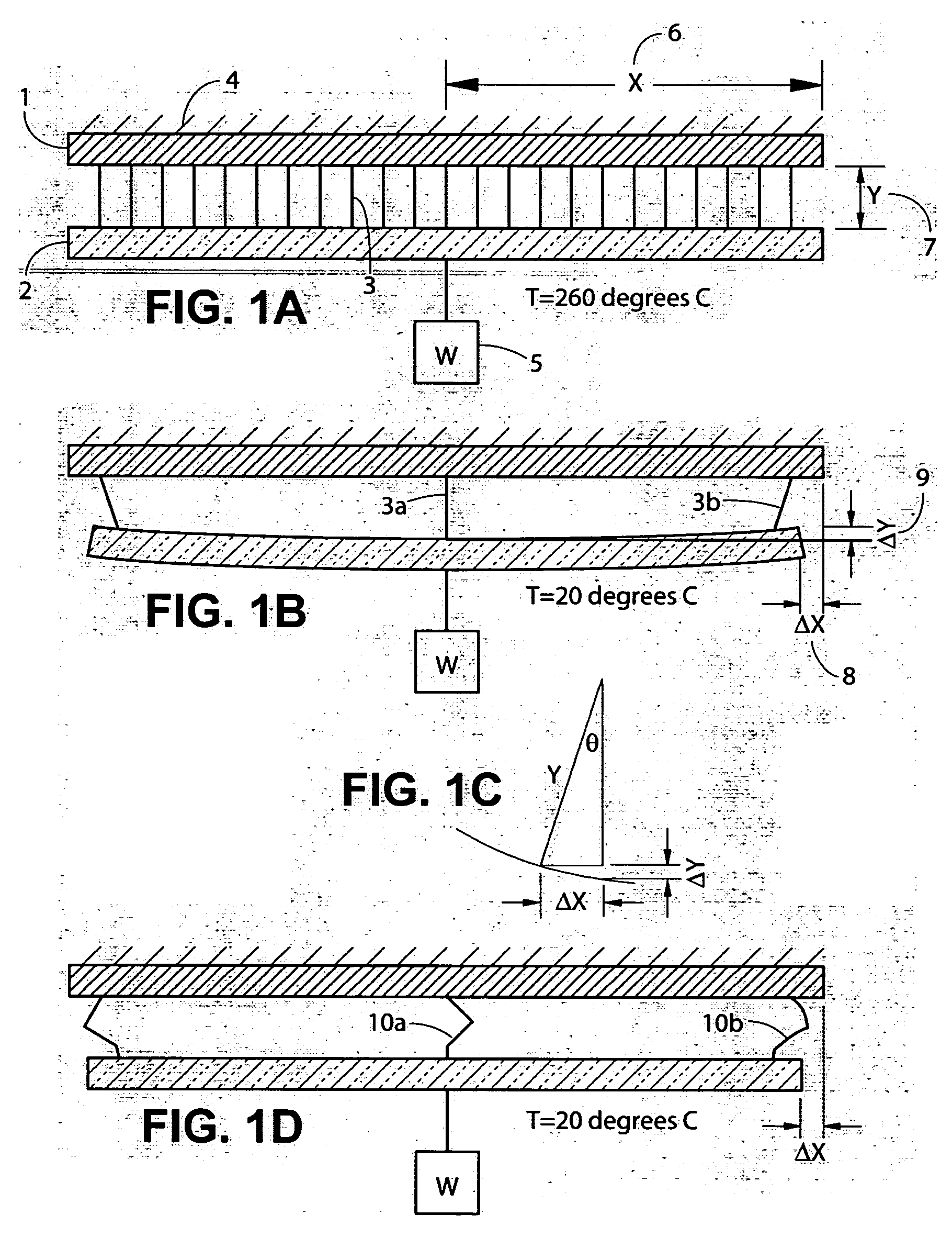
The attachment between chip and substrate comprising an array of such spheres is stiff rather than compliant.
Since semiconductor materials expand and contract at slower rates than typical substrates, temperature excursions cause shear forces to develop at the interface between chip and substrate.
The shear stresses may cause buckling, cracking or de-lamination.
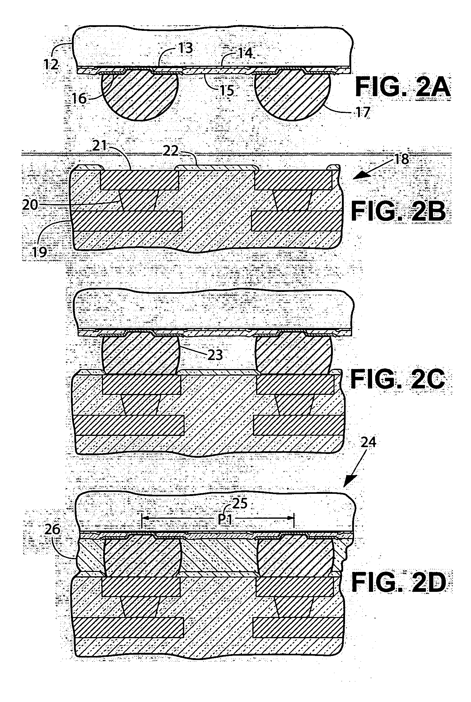
However, if an epoxy under-layer is used, it is almost impossible to rework an assembled die that proves to be defective.
However, thermal grease is not conductive enough to meet the heat-sinking requirements projected for 2010.
This limitation severely constrains how wire-bonded chips can b

Method used


Image

  • Repairable three-dimensional semiconductor subsystem
  • Repairable three-dimensional semiconductor subsystem
  • Repairable three-dimensional semiconductor subsystem

Examples


embodiment 90

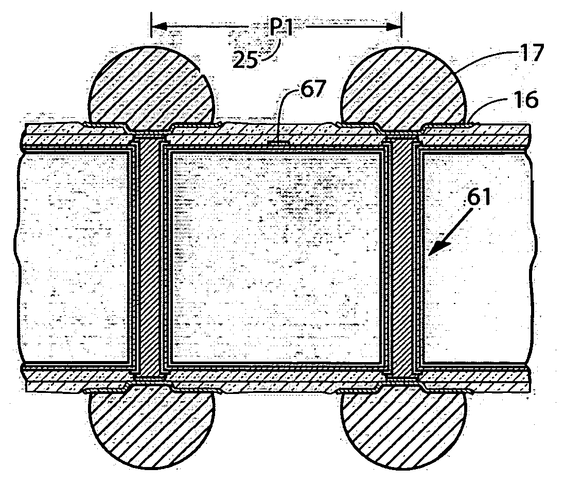
[0063]FIG. 7A illustrates a second preferred embodiment 90 of a repairable electronic subsystem of the current invention. In addition to the elements of subsystem 70 of FIG. 6A, subsystem 90 includes a heat sink 91 attached using interface adaptor 52. Attachment at interface 93 may be accomplished using a thin film of thermally conductive epoxy for example. Reactive foils may also be used to melt a sheet of solder at the interface, thereby bonding the parts together with low thermal impedance. Heat sink 91 may be an enclosure that also serves as a heat sink. Preferably heat sink or enclosure 91 provides strong mechanical support as well as heat extraction. Additional IC chips such as 92 are attached to the top side of integration platform 72b, which now includes through wafer connections like 61 of FIGS. 5A and 5B, in order to connect between semiconductor elements on its top and bottom sides.

embodiment 95

[0064]FIG. 7B illustrates a third preferred embodiment 95 of a repairable electronic subsystem of the present invention. Subsystem 95 includes another semiconductor integration platform 72c, connected using I / O plugs 60b to platform 72b of FIG. 7A. This provides mechanical and electrical support for another layer of IC chips such as 96 to be attached to the under side of platform 72c.

embodiment 100

[0065]FIG. 7C illustrates a fourth preferred embodiment 100 of a repairable electronic subsystem of the present invention. Subsystem 100 includes semiconductor integration platforms 71, 72b, and 72c each having attached semiconductor elements as shown. Unlike most electronic subsystems employing stacked semiconductor elements, complexity is not limited by yield issues but rather by thermal considerations. Accordingly, subsystem 100 includes interface adaptors at both top and bottom, 52b and 52, attached to heat sinks 101 and 91 as shown. This arrangement provides a thermal and electrical architecture that may support supercomputers of the future, including sets of parallel planes of heat sinks such as 101 and 91, with dense assemblies of semiconductor elements sandwiched in between as shown, connected using cables such as 76.

[0066]FIG. 8 is a schematic view of a semiconductor integration platform 110 of the current invention. Integration platform 110 incorporates examples of all of ...


PUM


Abstract

A tightly packed three-dimensional electronic system or subsystem comprising multiple stacks of semiconductor elements is described. The system is repairable because the elements connect together using re-workable flip chip connectors; each flip chip connector comprises a conductive spring element on one side and a corresponding well filled with solder on the other side. The spring elements relieve stresses at the interfaces and allow the component stacks to remain flat; they also provide vertical compliance for easing assembly of elements that have been imperfectly thinned or planarized. Semiconductor integration platforms may be used to integrate active and passive devices, multi-layer interconnections, through wafer connections, I/O plugs, and terminals for attachment of other semiconductor elements or cables.

Description

[0001] This invention relates to methods for integrating electronic systems or subsystems, and more particularly to a repairable three dimensional electronic subsystem wherein semiconductor elements are closely packed and can be replaced if they prove to be defective. BACKGROUND OF THE INVENTION [0002] A common form of electronic subsystem includes a printed circuit board (PCB) with multiple packaged components assembled onto the board, wherein each packaged component includes a semiconductor chip or die. As the clock rate of electronic subsystems has increased, it has become desirable to make smaller and smaller packages. The smaller packages typically have shorter lead lengths with lower inductance, and the lower inductance enables higher speed operation. Flip-chip packages represent an extension of this trend, comprising bumped die directly attached to a package substrate or PCB. The bumps have typically been solder balls arranged in ball grid arrays (BGAs). [0003] BGA attachment...

Claims


Application Information

Patent Timeline
IPC IPC(8): H01L23/04H01L23/48
CPCH01L21/4853H01L2224/11332H01L23/147H01L23/36H01L23/49811H01L23/49827H01L23/66H01L24/11H01L24/12H01L24/16H01L24/72H01L24/81H01L25/0652H01L2224/1147H01L2224/11474H01L2224/11554H01L2224/11901H01L2224/13099H01L2224/16H01L2224/81052H01L2224/81101H01L2224/81121H01L2224/81193H01L2224/8121H01L2224/81815H01L2225/06517H01L2225/06575H01L2924/01013H01L2924/01022H01L2924/01027H01L2924/01029H01L2924/01047H01L2924/01074H01L2924/01075H01L2924/01078H01L2924/01082H01L2924/14H01L2924/19041H01L2924/19043H01L2924/30105H01L2924/30107H01L2924/3011H01L2924/01005H01L2924/01006H01L2924/01019H01L2924/01023H01L2924/01033H01L2924/0105H01L2924/014H01L2924/00013H01L21/6835H01L2924/3651H01L2224/131H01L2224/81191H01L2224/16237H01L2224/29099H01L24/05H01L24/13H01L2224/0401H01L2224/05001H01L2224/05022H01L2224/0557H01L2224/05571H01L2224/05647H01L2224/05666H01L2924/00014H01L2924/15747H01L2924/351H01L2924/00H01L2224/05099
Inventor SALMON, PETER C.
Owner IP3 2022 SERIES 922 OF ALLIED SECURITY TRUST I
Why Eureka
Try Eureka