

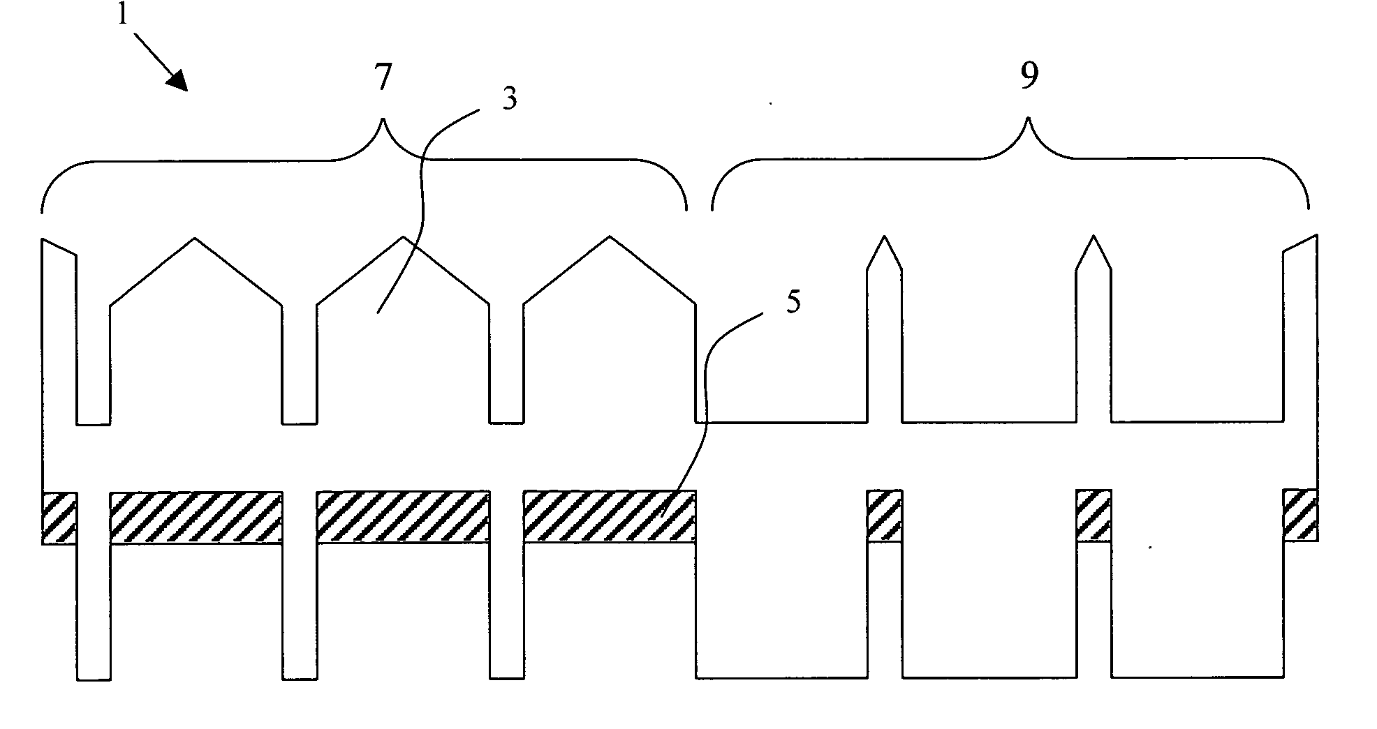
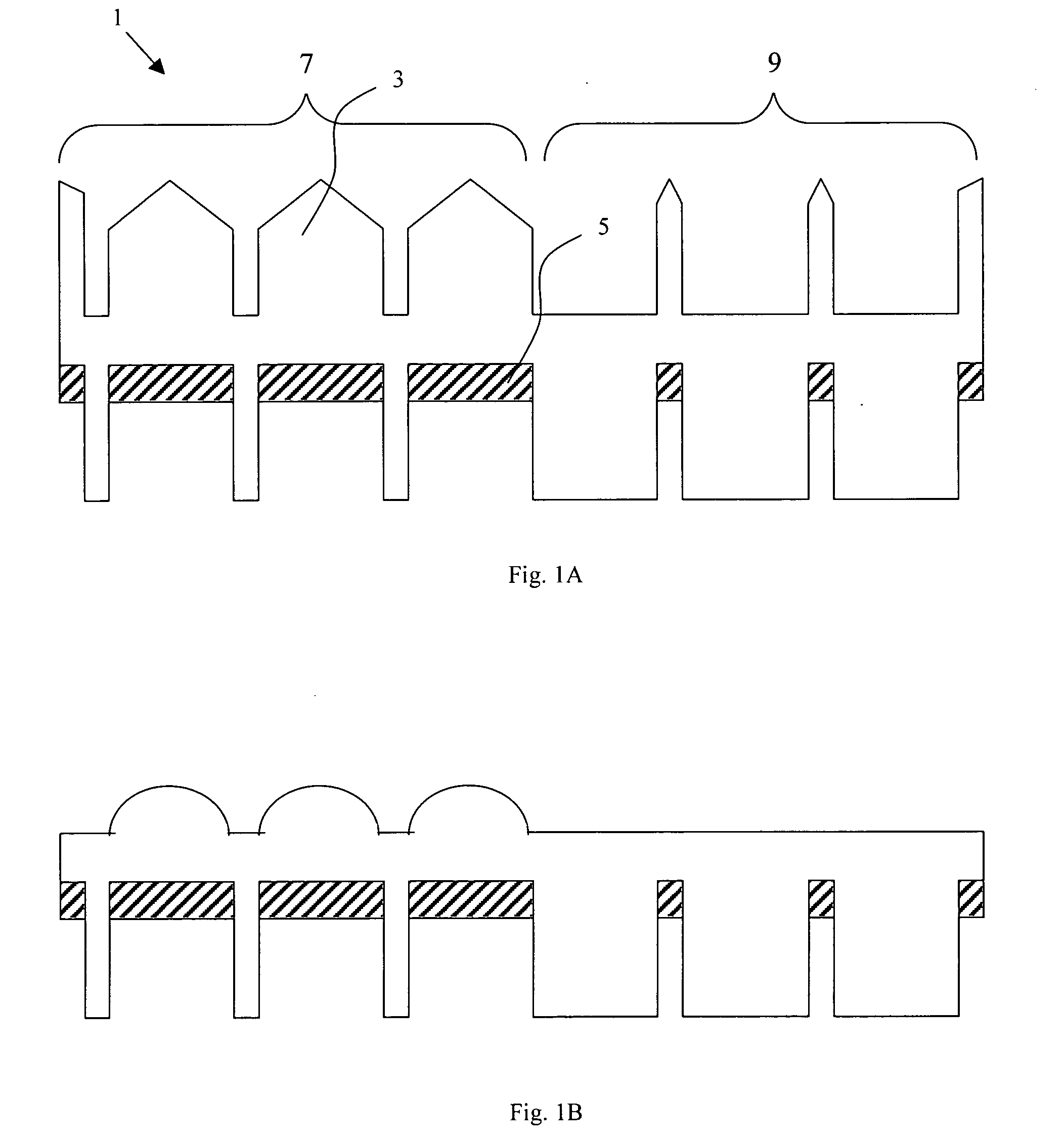
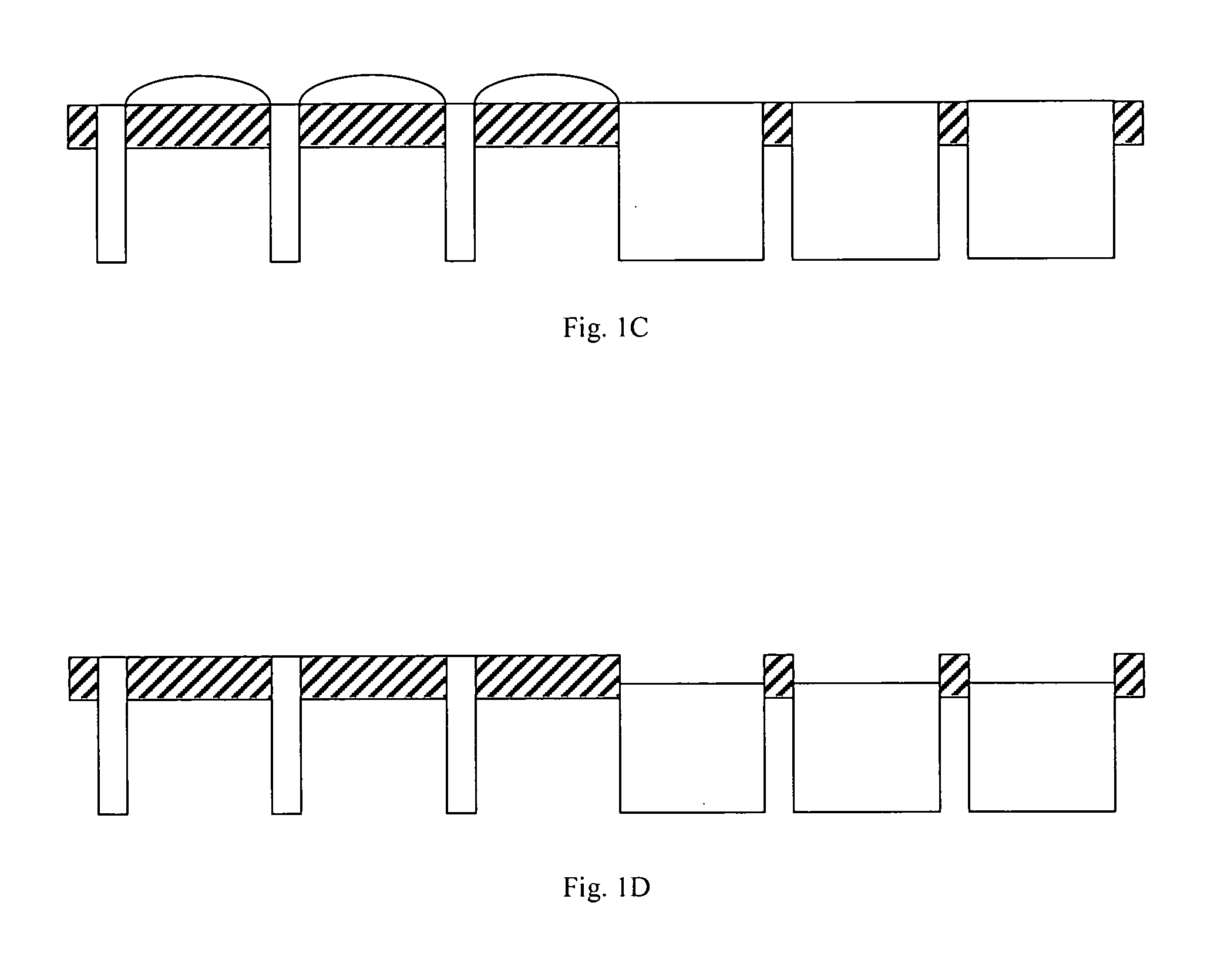
Multi-step methods for chemical mechanical polishing silicon dioxide and silicon nitride
a technology of silicon nitride and silicon dioxide, which is applied in the direction of other chemical processes, semiconductor/solid-state device testing/measurement, instruments, etc., can solve problems such as die scale thickness variations
- Summary
- Abstract
- Description
- Claims
- Application Information
AI Technical Summary
Benefits of technology
Problems solved by technology
Method used
Image

Examples
example 1
[0047] This experiment measured the planarization performance of the two step polishing method compared to a single step process for trench oxide planarization. In particular, the effect of the two step polishing method on dishing in 10% to 90% trench oxide was tested. A 10% trench oxide is defined herein as the trenches in an array of repeated structures wherein the active width / (trench width+active width)×100%=10%. For example, if the trench width+active width=100 microns, the 10% trench has a width of 90 microns. Similarly, the 90% trench has a width of 10 microns. For the single step process, an Applied Materials Mirra 200 mm polishing machine using an IC1000™ polyurethane polishing pad (Rohm and Haas Electronic Materials CMP Inc.) under downforce conditions of 2.7 psi and a polishing solution flow rate of 85 cc / min, a platen speed of 123 RPM and a carrier speed of 44 RPM planarized the samples. For the first of the two step process, an Applied Materials Mirra 200 mm polishing m...
example 2
[0049] This experiment measured the planarization performance of the two step polishing method compared to a single step process nitride planarization. In particular, the effect of the two step polishing method on nitride loss in 10% to 100% site feature was tested. The process conditions were the same as that of Example 1.
TABLE 2Center DieMiddle DieEdge DieGlobalSiteNitrideNitrideNitrideNitrideFeatureThicknessThicknessThicknessThicknessTest(%)Range (Å)Range (Å)Range (Å)Range (Å)B10-100210162172210210-10041254158
[0050] As illustrated in Table 2 above, the two step process (Test 2) provided significantly less nitride loss in low density features as compared to the single step process (Test B). Each of the nitride thickness ranges of the center, middle and edge die for the single step process provided a much greater range than that of the two step process. Namely, the nitride thickness ranges for the center, middle and edge die were 210 Å, 162 Å and 172 Å, respectively, for the sing...
PUM
| Property | Measurement | Unit |
|---|---|---|
| Molar mass | aaaaa | aaaaa |
| Molar mass | aaaaa | aaaaa |
| Molar mass | aaaaa | aaaaa |
Abstract
Description
Claims
Application Information