
MEMS device package and method for manufacturing the same

a technology of micro electromechanical system and device package, which is applied in the direction of microstructural technology, semiconductor devices, electrical equipment, etc., can solve the problems of limiting the size of the package, affecting the miniaturization of the apparatus, and difficult to perform, so as to reduce the stress and minimize the size

Inactive Publication Date: 2006-06-29
SAMSUNG ELECTRONICS CO LTD
View PDF6 Cites 4 Cited by
  • Summary
  • Abstract
  • Description
  • Claims
  • Application Information

AI Technical Summary

Benefits of technology

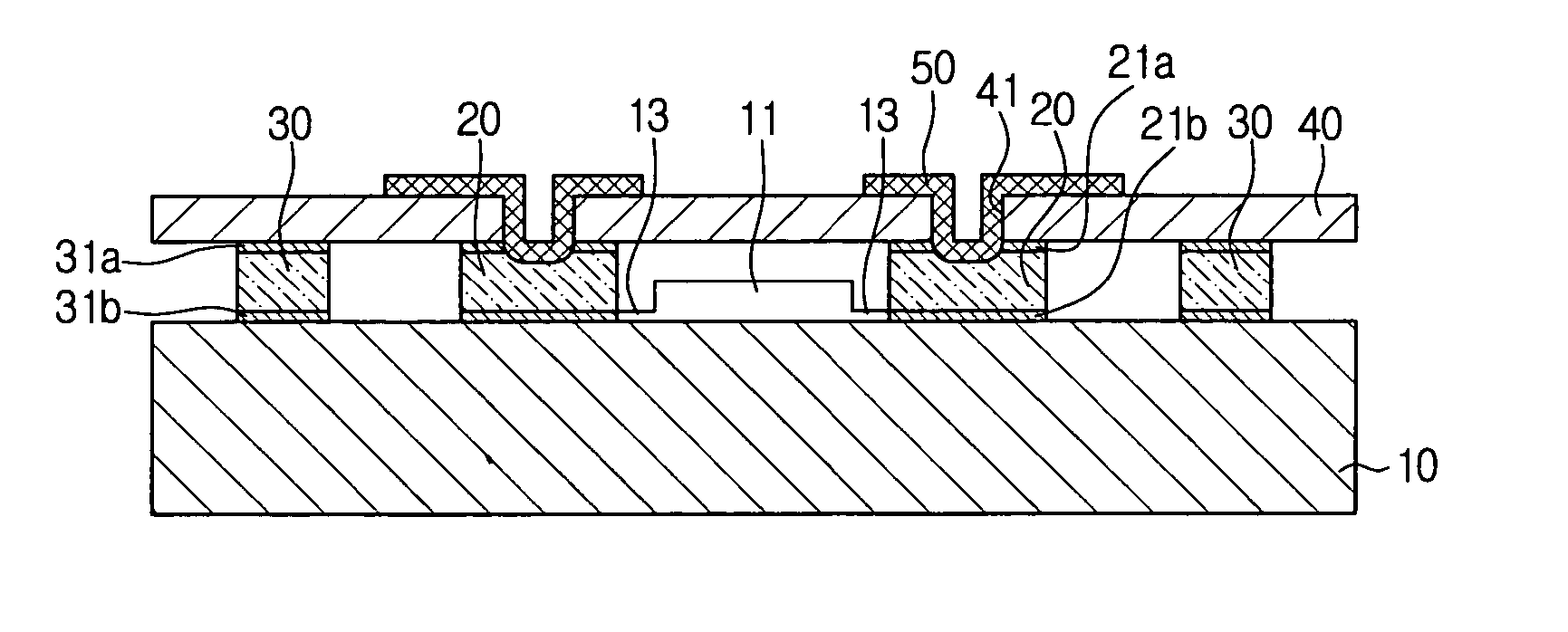
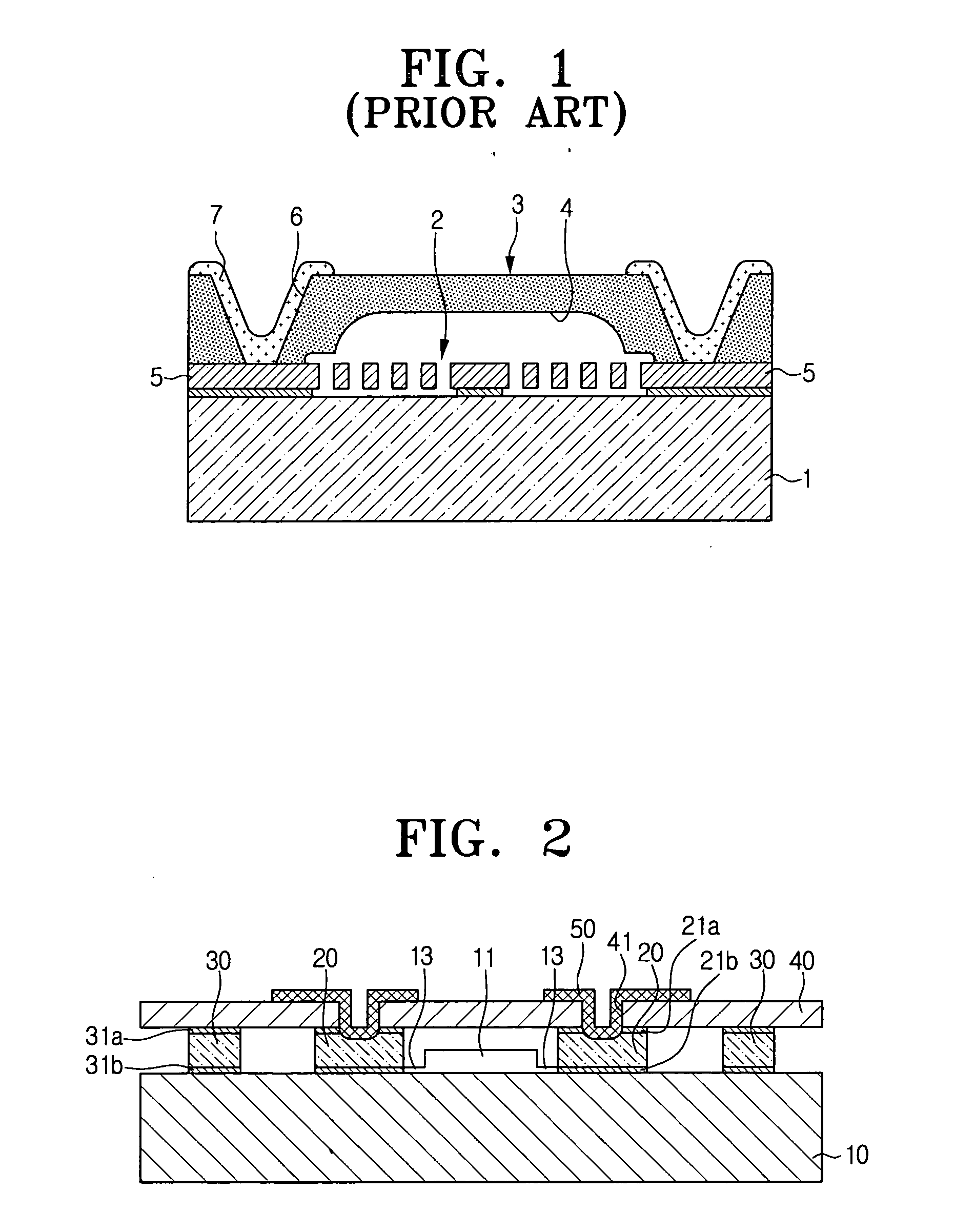
[0014] Accordingly, an illustrative, non-limiting embodiment of the present invention has been made to solve the above-mentioned problems, and an aspect of the present invention is to provide a MEMS device package, in which a closure substrate formed from a material identical to that of a device substrate is employed so as to reduce the stress caused by a difference in thermal expansion coefficient, and in which via holes for wiring of electrodes can be simply fabricated and a simple metal deposition process can be employed, so that the MEMS device package can be minimized in size, and a method of manufacturing such a MEMS device package.
[0016] A still further aspect of the present invention is to provide a MEMS device package, in which a circuit connection structure is formed by contacting members formed from a same or highly conductive material so as to minimize the loss in signal, and a method of making such a MEMS device package.

Problems solved by technology

However, a conventional MEMS device package as described above inevitably has a thick glass closure substrate 3 due to the bonding structure between the glass closure substrate 3 and a silicon-based device substrate 1 and the manufacturing process of the MEMS device package, whereby there is a limit in reducing the size of the package due to the via holes 6 in the glass substrate 3.
In other words, due to a large size and a high height, such a conventional MEMS package occupies a large volume in an apparatus incorporating it, thereby causing the miniaturization of the apparatus to be hindered.
Furthermore, because such a conventional MEMS package employs a closure substrate 3 formed from glass, the processes for forming the via holes 6 and the external electrode pads 7 are difficult to perform and require much time, thereby causing a decrease in yield and productivity.
Such a conventional MEMS package also has a problem in that the MEMS active device 2 may be deformed or damaged due to high temperature (typically about 460° C.) at the time of anodic-bonding and has basic stress due to the difference in thermal expansion coefficient between the glass closure substrate 3 and the silicon-based device substrate 1.
Moreover, a problem of reliability may be presented because the connection of a circuit by means of the internal electrode pads 5 formed from a silicon material and the external electrode pads 7 formed from a metallic material produces a very high inductance in relation to RF signals of high frequency and electrical contact resistance at the contact parts, thereby causing a high loss in signal.

Method used


Image

  • MEMS device package and method for manufacturing the same
  • MEMS device package and method for manufacturing the same
  • MEMS device package and method for manufacturing the same

Examples


Embodiment Construction

[0030] Hereinbelow, an exemplary embodiment of the present invention is described in detail with reference to accompanying drawings.

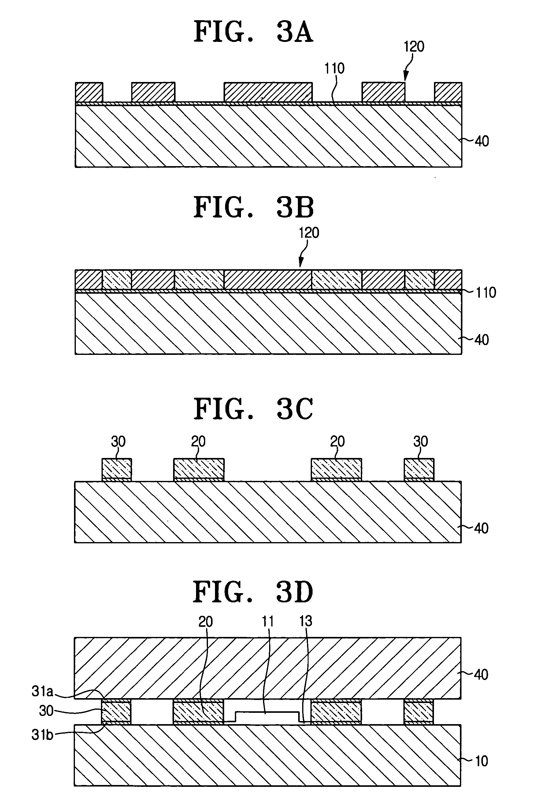
[0031]FIG. 2 is a schematic structural view of a MEMS device package according to an exemplary embodiment of the present invention. As shown in the drawing, a MEMS active device 11 is formed on the central part of the top surface of a device substrate 10. The MEMS active device 11 typically comprises a spring element, a stage supported by the spring element and electrodes for detecting the displacement of the stage or supplying a driving force for the stage. Such a MEMS active device 11 does not limit the technical scope of the present invention. In addition, lead lines 13 electrically connected to the MEMS active device 11 are formed on the device substrate 10.

[0032] Internal electrode pads 20 having a predetermined height are placed on the device substrate 10, wherein each of the internal electrode pads 20 is positioned on the opposite side of the M...


PUM


Abstract

A micro electromechanical system (MEMS) device package and a method of manufacturing the same are provided. The MEMS device package includes: a device substrate with a MEMS active device being formed on the top surface thereof; internal electrode pads, each of which is positioned on the opposite side of the MEMS active device and electrically connected to the MEMS active device; sealing pads positioned outside of the internal electrode pads; a closure substrate joined to the device substrate through the sealing pads, the closure substrate having via holes formed at the areas where the internal electrode pads are positioned; and external electrode pads formed on the top surface of the closure substrate in such a way that the external electrode pads are electrically connected to the internal electrode pads through the via holes. The internal electrode pads and the sealing pads are formed from an identical material such as Au and thus the device substrate and the closure substrate are bonded to each other with direct bonding such as Au—Au direct bonding via the sealing pads.

Description

CROSS-REFERENCE TO RELATED APPLICATIONS [0001] This application claims priority from Korean Patent Application No. 2004-112700 filed Dec. 27, 2004 in the Korean Intellectual Property Office, the disclosure of which is incorporated herein by reference. BACKGROUND OF THE INVENTION [0002] 1. Field of the Invention [0003] Apparatuses and methods consistent with the present invention relate to a micro electromechanical system (MEMS) device package and a method for manufacturing the same. [0004] 2. Description of the Related Art [0005] MEMS is the integration of sensors, micro actuators, gyroscopes, precise machine parts, etc. using semiconductor processing technology. As a high level of precision, product uniformity, and superior productivity required for semiconductor processing are applied to MEMS, MEMS is recognized as a technology capable of improving performances of products while reducing costs. [0006] MEMS devices such as acceleration sensors, angular velocity sensors, resonant gy...

Claims


Application Information

Patent Timeline
Patent Type & Authority Applications(United States)
IPC IPC(8): H01L21/00
CPCB81B7/007H01L29/00
Inventor KIM, JONG-SEOKPARK, YUN-KWONSONG, IN-SANGKIM, DUCK-HWANNAM, KUANG-WOOYUN, SEOK-CHUL
Owner SAMSUNG ELECTRONICS CO LTD
Learn More